 |
|
||||
BiographyMauro Borghi was born in 1995 in Reggio Emilia, Italy. He completed his Bachelor's Degree in Mechanical Engineering and Master's Degree in Materials Engineering from the University of Modena and Reggio Emilia. He performed his thesis work at Helmut Schmidt University, Hamburg. He joined the Institute for Microelectronics in 2022, where he is working on the growth and characterization of fluorides for 2D nanoelectronics in collaboration with the University of Modena and Reggio Emilia. |
|||||
Preliminary Investigation of LaF₃ as a Gate Insulator for FETs
Lanthanum fluoride (LaF3) is a wide-bandgap ionic crystal with a high dielectric constant (ε ≈ 13 to 17) and self-passivated by chemically inert, fluorine-terminated surfaces. These properties make it a promising candidate for gate insulators in field-effect transistors (FETs), particularly in device architectures requiring clean van der Waals interfaces with two-dimensional materials.
Thin films of LaF3 were deposited using molecular beam epitaxy (MBE) under ultra-high vacuum conditions. A systematic study of the deposition temperature was carried out to assess its influence on film crystallinity, interface quality, and surface morphology. Silver single crystals with (111) orientation [Ag(111)] were selected as the conductive substrate: the use of a conductive substrate is functionally relevant, as it enables, in principle, the implementation of a back-gate configuration in field-effect transistor architectures.
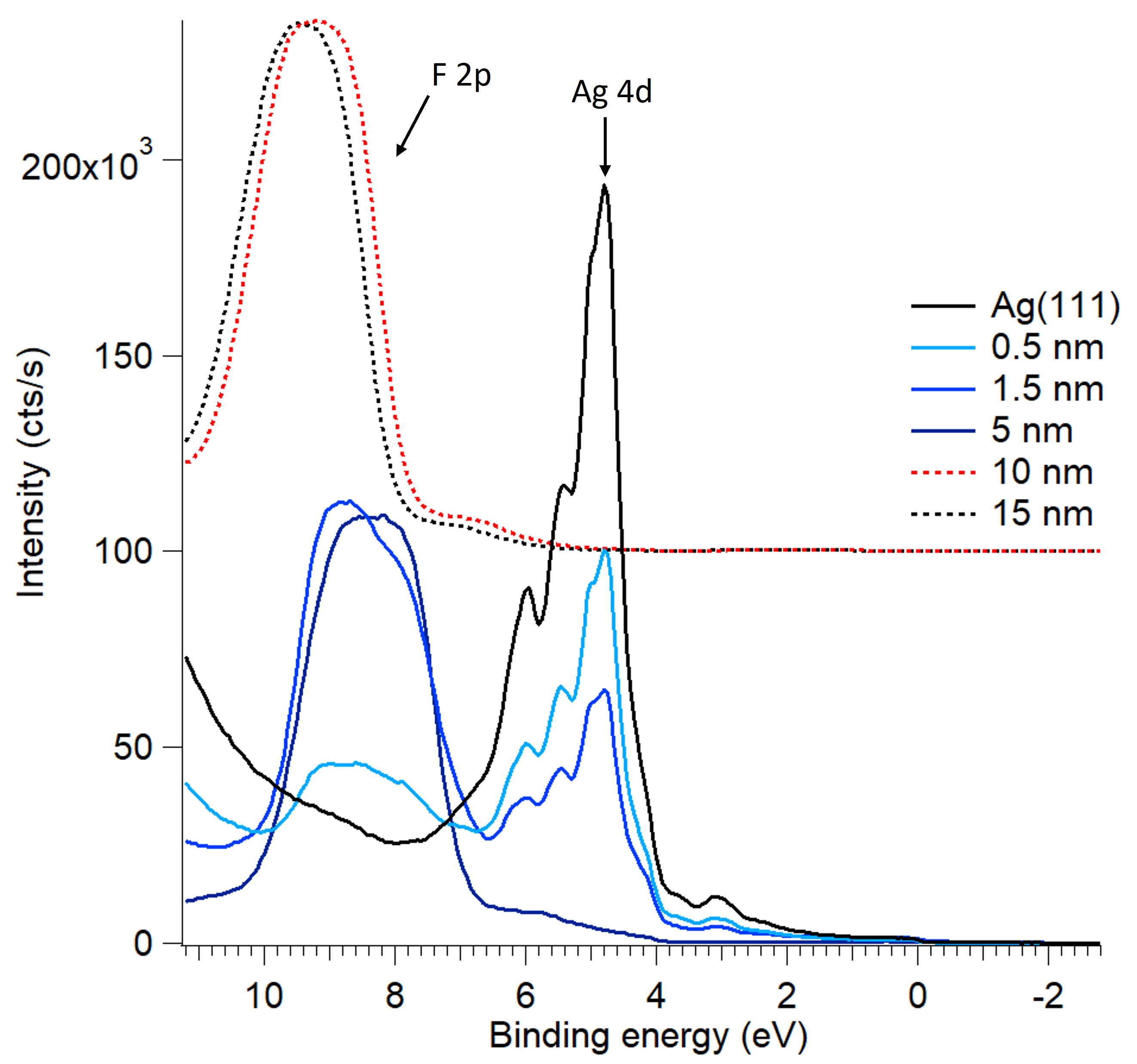
Surface-sensitive characterization techniques were employed to evaluate the properties of the deposited films. X-ray photoelectron spectroscopy (XPS) and ultraviolet photoelectron spectroscopy (UPS) were used to investigate the chemical composition and electronic structure. Low-energy electron diffraction (LEED) provided information on surface crystallinity after growth. Atomic force microscopy (AFM) was used to assess surface morphology and roughness at the nanoscale.
The results highlight the central role of substrate temperature during deposition. When all other growth parameters are kept constant, temperature strongly affects both the surface diffusion kinetics of the evaporated species and can promote chemical reactions at the film interface. This dual influence impacts the structural and electronic quality of the resulting LaF3 layers, confirming the need for precise thermal control during growth to achieve optimal film characteristics for device integration.

Fig. 1: AFM images after the deposition of 5 nm of LaF3 at room temperature (left image) and at 400°C (right image) in morphology contrast. In the RT deposition, the characteristic step-terrace structure of the Ag(111) substrate remains clearly visible. This indicates that while the fluoride film uniformly covers the surface, the limited surface mobility of the molecules prevents them from effectively crossing the step edges, resulting in a LaF3 accumulation at these boundaries. In contrast, deposition at 400 °C results in the formation of distinct, three-dimensional islands rather than a continuous film. The increased kinetic energy at this temperature enhances the surface diffusion of the evaporated species, favoring nucleation and aggregation into separate structures. This behavior reflects a temperature-induced transition in growth dynamics.


