 |
|
||||
BiographyAlexander Karl rreceived his Bachelor and Master degrees in Technical Physics from TU Wien in 2020 and 2022, respectively. For his Master's thesis he focused on the search for Dark Matter with the CRESST experiment. In August 2022 he joined the Institute of Microelectronics and is pursuing his PhD studies. Currently, his research is focused on the modeling of 2D field effect transistors using, e.g., the compact physics framework Comphy, and on investigating the application of novel 2D materials towards the realization of electronic devices. |
|||||
Comphy 4.0: Accelerating 2D-MOSFET Reliability Studies
Metal oxide semiconductor field effect transistors (MOSFETs) remain foundational to integrated circuit performance. Recent breakthroughs in two-dimensional materials, like transition metal dichalcogenides, offer atomically thin channels that promise further device scaling and efficiency. Yet 2D-MOSFET prototypes often suffer from stability and reliability issues under real-world conditions, so to leverage their full potential we must uncover the physical mechanisms driving these instabilities.
To address this need, we developed Comphy, a Python framework for simulating key reliability phenomena in MOSFETs. Comphy’s core modules model hysteresis effects, bias temperature instability, and tunneling currents, factors that govern device aging and leakage. Users can explore how charge trapping, interface states, and leakage pathways evolve across various bias and thermal profiles.
Enhancing the original codebase, we first incorporated full support for two-dimensional materials, enabling accurate reliability analyses of MoS₂, WSe₂, and other layered semiconductor transistors. This involved revising the electrostatic solver and calibrating against experimental data to ensure the accuracy of the new models.
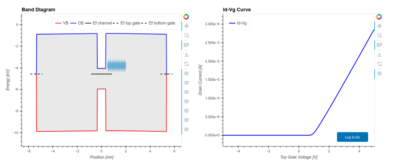
Next, to make Comphy accessible to newcomers, we built an intuitive graphical user interface (GUI). The GUI walks users through device parameter selection, simulation setup, and results visualization, automatically generating plots of the threshold voltage, hysteresis, and tunneling currents over time. This front end streamlines benchmarking and comparison tasks, empowering researchers without deep Python or command-line expertise.
Together, these enhancements transform Comphy into a versatile, user-friendly platform for both conventional silicon-MOSFET reliability studies and cutting-edge investigations of 2D-material devices, accelerating semiconductor reliability research and design.

Fig. 1: Comphy's graphical user interface that allows the user to select device parameters, configure the simulation setup, and visualize the simulation results.


