 |
|
||||
BiographySabine Leroch obtained her M.Sc. and doctoral degrees at TU Wien at the Institute of Theoretical Physics, after which she took a post-doctoral position at the Universidad Compludense de Madrid. She has many years of experience in classical molecular dynamic simulations in different fields and for a broad set of applications. She was previously employed as a post-doctoral researcher at the University of Natural Resources and Applied Life Sciences (BOKU) Vienna, in the field of bio-chemical engineering and as senior scientist at the Austrian Competence Center of Tribology. At the Institute for Microelectronics, Sabine is working in the Christian Doppler Laboratory for Multi-Scale Process Modeling of Semiconductor Devices and Sensors, where she is in charge of the atomistic description of physical processes taking place during the fabrication of semiconductor devices. In particular, she is investigating the implantation and activation of dopants in silicon carbide (SiC). |
|||||
Temperature and dose dependent annealed defect structures in shallow Al-implanted 4H-SiC
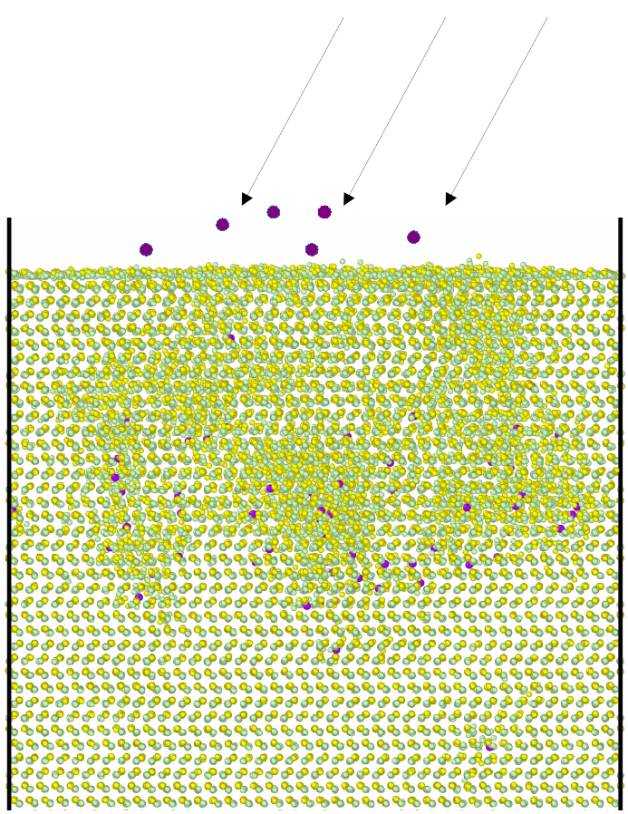
Depending on the implantation conditions such as ion dose or wafer temperature, isolated point defects can occur, but also extended defect clusters up to amorphous pockets. Subsequent high-temperature annealing is necessary to reduce the number of defects. In a previous MD study, we observed that the allocation of Al on silicon lattice sites at doses above the saturation limit is lower for high wafer temperatures than for lower ones. We therefore investigated the dynamic processes that take place during defect annealing in more detail.
Defect structures for two implantation temperatures 500 and 900 K and 7 doses (0.5-7.5 x 10¹⁴cm⁻²) were analyzed systematically. It was found that small stable (Al-C) complexes consisting of two to three defects as shown in Fig.1(a-b) remained at the end of annealing in all systems. At high doses, increasingly larger defect clusters consisting of aluminum and residual interstitials were formed during annealing, with a clear dependence on the implantation temperature. While a larger number of smaller clusters predominated at 500 K, at 900 K there were only a few extended defects that could grow into dislocation loops shown in Fig.1(c-d).
Cluster sizes and concentrations as a function of implantation dose and temperature are shown in Fig.1(e). Extended defects acted as sinks for diffusing interstitials and dopants and therefore have an influence on dopant activation. In agreement with experiments, the activation directly after implantation at 500 K is low as can be seen in Fig.1(f), but increases sharply after annealing. At 900 K, a higher concentration of acceptor Al is already present after implantation, but this hardly changes in the subsequent annealing. A possible explanation for this is that during epitaxial regrowth of amorphous pockets formed at 500 K, the incorporation of Al into the SiC lattice is enhanced, while at 900 K the dopants are rather bound by interstitial clusters.

Fig. 1: Top: Small (Al-C) complexes found at the end of the annealing process: Shown here are the stable Aluminum-Dicarbon complex (a), and the Aluminum Carbon-antisite split interstitial located at the silicon site (b). Extended defect: shown is a dislocation loop in the center of the figure, surrounded by an Al-Si-C precipitate in (c). In (d) one can see a side view of the same dislocation to visualize the additional layer that was inserted into the stacking sequence of 4H-SiC. Crystalline Silicon is shown in light gray, Carbon in dark gray, defects such as Silicon and Carbon interstitials are shown in green and blue, anti-sites in cyan, while acceptor Aluminum is red and aluminum interstitials are brown. Bottom: Defects in dependence of implantation temperature and dose e) Maximum number of clusters and cluster size. f) Aluminum at lattice sites before (solid) and after annealing (dashed) at 2350 K. g)Concentration of acceptor Aluminum together with compensating defects.


