 |
|
||||
BiographyTobias Reiter obtained his Master's degree (Dipl.-Ing.) in Technical Physics in 2022 and is currently completing the inter-faculty Master Program (MSc.) Computational Science and Engineering, both at TU Wien. He joined the IµE as a doctoral candidate in 2022, where he is working on semiconductor process simulation. His current research focuses on the development of the process simulation library ViennaPS, where he is developing models for novel etching and deposition processes for semiconductor fabrication. He is also part of the Christian Doppler Laboratory for Multi-Scale Process Modeling of Semiconductors Devices and Sensors. |
|||||
Physical Insights into Ion Beam Etching from a Calibrated Simulation Framework
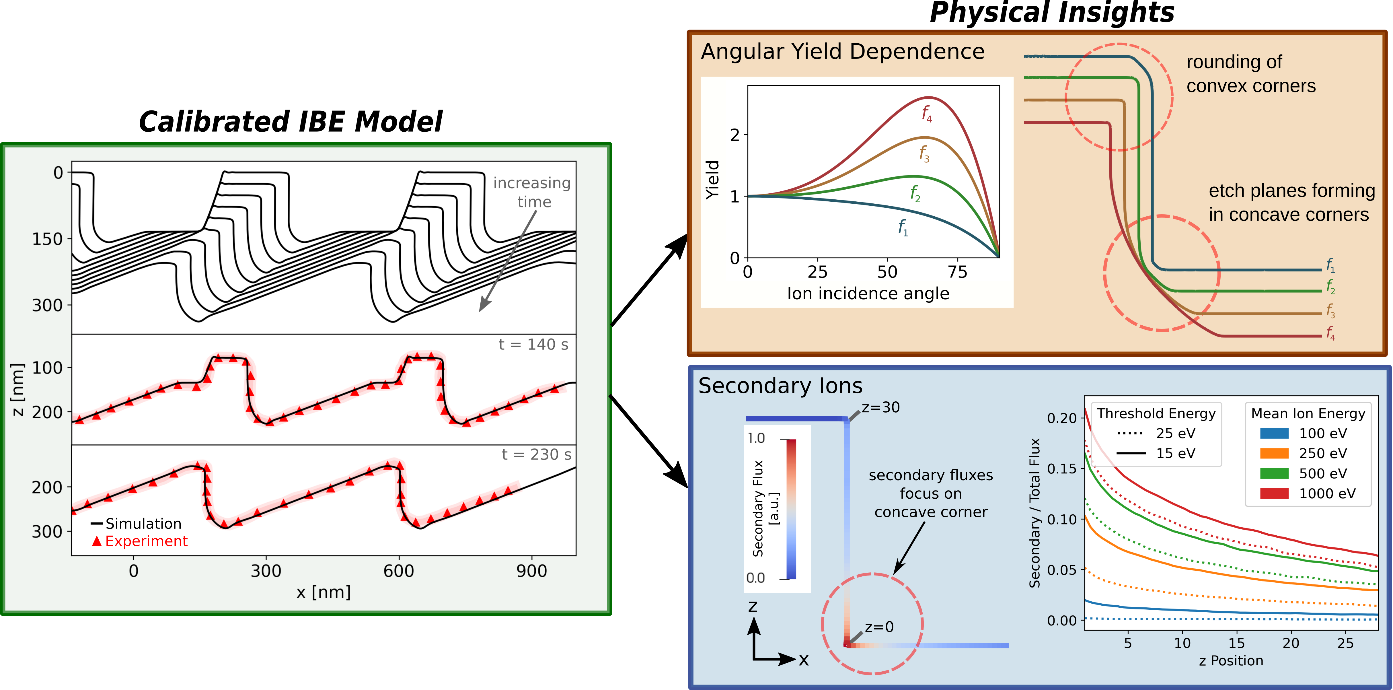
Ion beam etching (IBE) is a widely used technique for fabricating high-precision micro- and nanostructures, such as blazed gratings in optoelectronic devices. Our research has focused on developing physically grounded models for oblique-angle IBE that accurately capture complex surface evolution. These models integrate Monte Carlo ray tracing to simulate ion trajectories with level-set methods for tracking evolving surface geometries, accounting for energy- and angle-dependent sputtering yields as well as realistic surface reflections.
The simulation approach has been applied to reproduce multi-step angled etching processes observed in experiments, such as the formation of triangular blazed profiles from photoresist-patterned substrates. By calibrating the model against measured geometries, it becomes possible to explore the influence of beam parameters and material responses on etch profile development.
One of the key findings is the central role of the angular sputtering yield function in determining etch anisotropy and feature sharpness. Convex corners may remain well-defined or become rounded depending on the angular yield behavior, while in concave regions, the same function governs the emergence or suppression of new etch planes. Surface reflections give rise to secondary ion fluxes, which tend to accumulate in recessed areas and enhance local etch rates. This secondary flux plays a critical role in shaping sharp or asymmetric features and is strongly modulated by the primary ion energy.
Overall, our simulation framework and developed models provide valuable insights into the fundamental mechanisms governing IBE and supports the optimization of process parameters for advanced microfabrication applications.

Fig. 1: A calibrated simulation model for oblique ion beam etching is used to gain physical insight into microstructure formation, specifically for blazed gratings. The model captures energy- and angle-dependent sputtering as well as ion reflections, allowing detailed analysis of how process parameters affect etch profiles. It reveals how angular yield variations and secondary fluxes influence the evolution of convex and concave corners, providing guidance for precise process control.


