
 |
|
Biography
Oskar Baumgartner was born in Krems an der Donau, Austria, in 1982. He studied electrical engineering at the Technische Universität Wien, where he received the degree of Diplomingenieur in January 2007. He joined the Institute for Microelectronics in February 2007, where he is currently working on his doctoral degree. His scientific interests include the modeling and simulation of quantum transport in optical and nanoelectronic devices.
Direct Tunneling and Gate Current Fluctuations
Due to the continuing miniaturization of Metal-Oxide-Semiconductor (MOS) devices, fluctuations in the drain current increasingly affect device operation. This so-called Random Telegraph Noise (RTN) has been well studied and is now understood to consist of charge capture and emission events into and out of oxide defects. It has been recently reported that the fluctuations of the drain and the gate current can be correlated. Quite remarkably, the relative drop in gate current can reach up to 80% and is independent of temperature. Microscopically this means that the magnitude of the gate current is linked to the charge state of the oxide defects.
We carried out a comprehensive study of correlated gate leakage and drain current fluctuations in n-channel Metal-Oxide-Semiconductor Field-Effect Transistors (MOSFETs) using non-equilibrium Green’s function calculations. For that purpose a simulation model has been developed that combines 3D self-consistent electrostatic potentials accounting for random discrete dopants and charged oxide traps with a 1D and 2D transport description of direct-tunneling gate leakage. We investigated the influence of the charge state of the trap on the direct-tunneling current and observed a considerable local change in current density around the trap (see Fig. 1). By varying the position of the trap we found that oxide defects close to the drain and source regions have a higher impact on gate leakage. We carried out a statistical analysis of n-channel MOSFETs by varying the configuration of the random discrete dopants. The trap has been positioned close to the drain to achieve a worst-case scenario and we then calculated the reduction in direct-tunneling current due to charging of a single trap for each device. The gate current reductions predicted by the simulations were below one percent. Therefore, the experimentally measured large gate leakage fluctuations cannot be attributed to direct tunneling.
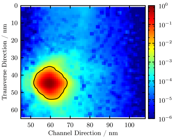
Fig. 1: Map of relative change in gate current density due to the charging of a trap for a particular doping and trap configuration. The map is constructed by a scan of 1D cuts over the whole gate area on a 1nm grid. The plot shows high local changes in the current around the position of the trap. The contour line corresponds to 1% of the maximum change in current. Its radius is below 10m and the current is therefore influenced only locally. The total change is calculated by integration over the whole area. Contrary to the high local change around the trap, the total reduction in gate current is small (below 1% per trap).
