
 |
|
Biography
Markus Bina was born in St. Pölten, Austria, in 1985. He studied electrical engineering at the Technische Universität Wien, where he received the degree of Diplomingenieur in 2010. He joined the Institute for Microelectronics in May 2010, where he completed his doctoral degree in 2013. In the same year, he also received his master's degree in biomedical engineering at the Technische Universität Wien. His current scientific interests include charge carrier transport, BTI, channel hot-carrier effects and variability in semiconductor devices as well as modeling of human bone structures using massive parallel finite element simulations.
Predictive Hot-Carrier Modeling of n-Channel MOSFETs
A physics-based hot-carrier degradation model which is based on the solution of the Boltzmann Transport Equation (BTE) using the deterministic solver ViennaSHE was developed. All modules of the Hot-Carrier Degradtion (HCD) model were incorporated within the same framework, namely on the platform of ViennaSHE. However, before solving the BTE, we employ the Sentaurus process simulator in order to reproduce the doping profiles as accurately as possible, since they affect the Energy Distribution Function (EDF). After the device simulator is calibrated in a manner to represent Id-Vd and Id-Vg characteristics of the pristine devices, the BTE solver is used to obtain the carrier EDFs for a particular device geometry and given stress or operating conditions (cf. Fig. 1). Next, this information is used to calculate interface state density profiles as a function of the coordinate along the semiconductor-insulator interface. Finally, these profiles are used to compute the characteristics of the degraded device for each stress condition over time. Using this approach, the model has been validated using a wide class of n-channel Metal-Oxide-Semiconductor Field-Effect Transistors (MOSFETs) with gate lengths of 65nm, 100nm, and 150nm. In this respect, it is important to emphasize that the model uses a unique set of parameters for all devices and stress conditions. Within this approach the consistent treatment of Si-H bond-breakage induced by a solitary hot carrier and bond rupture via excitation of the multiple vibrational modes has been performed. We therefore have considered all superpositions of the competing AntiBonding (AB) and Multiple Vibrational Excitation (MVE) processes. This means that the Si-H bond can be excited by a series of colder carriers to an intermediate level and then dissociated via excitation of one of the bonding electrons to an antibonding state by a single energetical carrier. Within this scenario the potential barrier separating this intermediate state and the transport mode is lowered due to the energetical position of the level. We have thoroughly analyzed the roles of the AB- and MVE-processes and realized that even in the case of ultra-scaled devices, the former plays the crucial role if the stress voltages are high. The role of Electron-Electron Scattering (EES) has also been studied in detail and it was shown that EES plays an important role in transistors with a gate length of 65nm and 100nm. Neglecting EES in these devices leads to a dramatic underestimation of HCD. At the same time, EES appears to be less important or even negligible in the 150nm MOSFET.
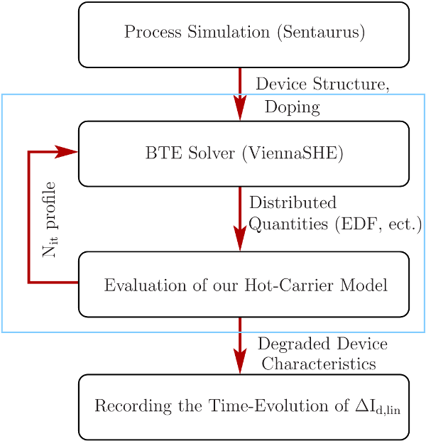
Fig. 1: Flow chart of the hot-carrier model evaluation. The first subtask is to simulate the device fabrication process using the Sentaurus process simulator. The last three subtasks have been integrated into our deterministic device simulator ViennaSHE: Solving the bipolar BTE, evaluation of our model and modeling of the degraded devices.
