
 |
|
Biography
Hajdin Ceric was born in Sarajevo, Bosnia and Herzegovina, in 1970. He studied electrical engineering at the Electrotechnical Faculty of the University of Sarajevo and the Technische Universität Wien, where he received the degree of Diplomingenieur in 2000. In June 2000, he joined the Institute for Microelectronics, where he received the doctoral degree in technical sciences in 2005 and where he is currently employed as a post-doctoral researcher. His scientific interests include interconnect and process simulation.
Electromigration Reliability of Solder Bumps
In recent years, a major paradigm change, from 2D IC to 3D Integrated Circuits (ICs), has taken place in the microelectronic industry. For the realization of modern 3D ICs, new interconnect structures, like Through Silicon Vias (TSVs) and solder joints/bumps, together with complex multilevel 3D interconnect structures, are gaining in importance. The application of these new structures unavoidably results in a rise of specific electromigration and stressmigration reliability issues. Solder bumps are important components for 3D integration because they enable vertical stacking of wafers and distribution of current supply (see Fig. 1). Failure of solder bumps has catastrophic consequences for the operating of ICs since it completely disturbs the current supply of wafers. Numerous experimental investigations have shown that solder bumps are very susceptible to electromigration and, to make thing worse, electromigration in solder bumps is much more complicated and much less investigated than electromigration in copper metallization. Pure Sn has been identified as the best material for ultra fine pitch solder bumps for advanced 3D interconnect applications due to its baseline advantages of being electrodeposited and exhibiting a low melting temperature.
An important part of the interconnect attached to the solder bumps is an Under Bump Metallization (UBM), which separates the Sn bump from the surrounding metallization. The solder bump with UBM has a lower maximum current density and peak temperature in the solder, which contributes to longer electromigration lifetimes. A solder bump interface to the UBM, which is usually made of Ni, enhances the development of alloys in solder bumps. At this interface, an Inter-Metallic Compound (IMC) is formed, which is a thin layer consisting of alloys with Sn as the principal component.
The current focus of my work is the development of models and simulation tools for a reliability analysis of solder bumps. The models encompass electromigration enhanced IMC formation, stability and dissolution of IMC and subsequent voiding and void evolution as a final stage of the failure of solder bumps. The simulation approach enables investigation of an influence of geometry and material variations on solder bump reliability and also helps to determine an optimal structure capable of resisting electromigration and mechanical degradation, and thus reduce failure probability.
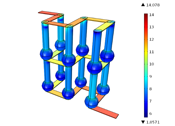
Fig. 1: Multilevel interconnect for 3D integration. Presented is the current density distribution on the logarithmic scale (x1000 A/cm²). Wafers are removed from the picture.
