
 |
|
Biography
Raffaele Alberto Coppeta was born in Torino, Italy, in 1986. He studied material engineering at the Politecnico of Torino, where he received the bachelor's degree in 2009 and the master's degree in 2011. He joined the Institute for Microelectronics in 2012, where he is currently working on his doctoral degree. His scientific interests include thermo-mechanical stress modeling using the finite element method for GaN-on-Si chips.
Modelling of the Residual Stress in III-N Film Grown on Si Substrate
Wurtzite stable forms of GaN and its alloys with aluminium or indium are considered the most important semiconductors since Si. Their direct bandgap, high breakdown field, high electron mobility, and sheet carrier density make them ideal for electronic devices operating at high frequencies and high temperatures, and for optical devices emitting bright light in a wide range of wavelengths.
Two important problems affecting the integration of GaN based alloys with Si are (1) cracks, created during the production process, and (2) a huge dislocation density that lowers carrier mobility, modifying the band structure, and relaxing the strain necessary to have the piezoelectric polarization.
Cracks are created during the cooling down from the typical epitaxial deposition temperature of the GaN based alloys on silicon substrate. Their formation is due to the big Coefficient of Thermal Expansion (CTE) mismatch between the GaN based alloys and Si. Analytical models based on continuum mechanics are used to determine the process and geometrical conditions at which cracks develop.
Dislocations are created due to the lattice mismatch at the interface between the GaN based alloy and Si, and additionally at the interfaces between the GaN and other alloys on top of it. Thermodynamical criterions and continuum mechanics are used to evaluate the film thickness at which the dislocations start to develop and then relax into two types of structures: superlattice and compositionally step graded structures.
In the scope of my work, the impacts of the anisotropy, the difference among the elastic properties of the alloys, their temperature dependence and the different slip systems of the dislocations are investigated. On the basis of these investigations new physical models are developed. The results obtained by using the new models show that the anisotropy and the difference between the elastic properties have a bigger impact on the equilibrium critical thickness of the GaN based alloys (see the Fig. 1) than in the SiGe one. There are two growth modes of GaN based alloys: the layer-by-layer growth mode, known as Frank-van der Merwe growth, and the island growth mode, known as Volmer-Weber growth. The impact of these two growth modes on the dislocation density and subsequent strain relief are currently investigated. The preliminary results show that the island growth mode lowers the dislocation density by an order of magnitude depending on the kinetic parameters of the epitaxial growth and the geometrical shape of the islands.
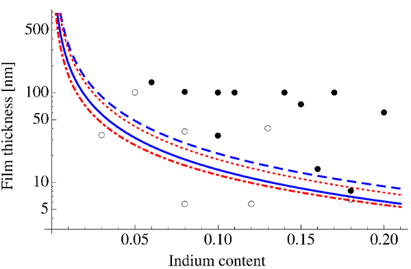
Fig. 1: The image shows the equilibrium critical thickness value for an InxGa1-xN film on GaN substrate as function of the indium content x, calculated according to the Freund-Suresh model (dashed lines) and the Steeds-Willis-Jain-Bullough model (solid lines) for two different dislocation slip systems (red and blue curve). The last one evaluate the impacts of the anisotropy and the appropriate elastic properties of the film and the substrate on the critical thickness. The filled points indicate the presence of misfit dislocations, while the empty points the absence. The crosses indicate the experimental critical thickness.
