
 |
|
Biography
Mahdi Pourfath was born in Tehran, Iran, in 1978. He studied electrical engineering at the Sharif University of Technology, where he received the MSc degree in 2002. He joined the Institute for Microelectronics in October 2003, where he received his doctoral degree in technical sciences in July 2007 and is currently employed as a post-doctoral researcher. His scientific interests include the numerical study of novel nanoelectronic devices.
Investigation of Graphene-Based Tunneling Field-Effect Transistors
Monolayer and bilayer graphene has been utilized as the channel material for Field-Effect Transistors (FETs), where the monolayer structure of graphene results in excellent gate control over the channel. The application of Graphene FETs (GFETs) for digital applications, however, is limited due to the absence of an energy bandgap. It is possible to induce an energy gap by patterning Graphene into NanoRibbons (GNRs). Fundamental problems of conventional GFETs have motivated researchers to focus on new structures, such as Tunneling FETs (TFETs). In these structures tunneling between source and drain is controlled by the gate-source voltage. In comparison with conventional FETs, TFETs have some advantages, such as having sub-threshold swings smaller than 60 mV/dec and relatively large on/off current ratios.
Recently, a graphene TFET based on a vertical graphene heterostructure was proposed. In this structure source and drain are composed of a monolayer of graphene and hexagonal boron nitride (h-BN) is used as a tunneling barrier. As shown in Fig. 1, the operation of this device is based on the voltage tunability of the density of states in graphene and of the effective height of the tunneling barrier. We have theoretically investigated device characteristics of Vertical Graphene TFETs (VTGFETs) and Graphene Nanoribbon TFETs (VTGNRFETs). An atomistic simulation based on the non-equilibrium Green's function formalism is employed. The results indicate that due to the presence of an energy gap in GNRs, the on/off-current ratio of VTGNRFET can be much larger than that of VTGFET, which renders VTGNRFETs as promising candidates for future electronic applications. Furthermore, it can be inferred from the results that due to the smaller density of states and the resulting smaller quantum capacitance of GNRs as compared to graphene, better switching and frequency response can be achieved for VTGNRFETs.
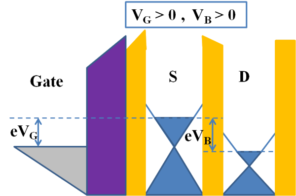
Fig. 1: The band structure of a VTGFET in the off state.
