
 |
|
Biography
Gerhard Rzepa, born in 1985 in Austria, studied at the Technische Universität Wien where he received the BSc degree in electrical engineering and the Diplomingenieur degree in Microelectronics in 2010 and 2013, respectively. He joined the Institute for Microelectronics in December 2013, where he is working on his doctoral degree. His current research topic is the microscopic modeling of oxide defects.
Microscopic Modeling of NBTI in MOS Transistors
Undesired effects in Metal-Oxide-Semiconductor (MOS) transistors, such as instabilities of their parameters and Random Telegraph Noise (RTN), can be traced back to charge exchange of oxides with the adjacent layers. In recent studies the capture and emission time constants of oxide defects have been successfully described on the basis of Non-radiative MultiPhonon (NMP) transitions. From this theory, the NMP four-state model, which considers two metastable states in addition to two stable states, emerged. These additional states are essential in order to capture the complex processes involved in Bias Temperature Instabilities (BTI) and RTN.
Depending on the geometry of the transistor, the number of oxide defects can be large. So, as the NMP four-state model describes each defect individually, the necessary number of parameters can become large as well. Suitable distribution functions for these parameters can be obtained with the help of measurement data (time dependent defect spectroscopy, threshold voltage degradation) and atomistic information about the defect sites (density functional theory). Once these distribution functions are available for a certain technology, the simulation with the NMP four-state model allows for very detailed insight into the ongoing processes. In addition to the temperature and bias dependence of the threshold voltage shift, quantities, such as the activation energy and Capture/Emission Time (CET) maps, can be computed (compare Fig. 1). The later turned out to be of particular interest, as these CET maps reveal effects related to the occupancy of the simulated defects. The occupancy of a defect can be independent from the stress conditions within a certain range of the gate voltage. This means that these defects do not contribute to device degradation for certain setups and therefore vanish in the corresponding CET maps. This has a significant effect on the shape of the distributions observed in CET maps and results in very specific gate voltage and temperature dependence. As the simulations allow for detailed investigations of these dependences, the NMP four-state model helped to explain previously unresolved observations of measured CET maps.
As the NMP four-state model covers the defects within the oxide, it has to be complemented by a model, which describes the creation of interface states in order to account for the more permanent component. The creation and annealing of interface states is described by a double well model while their charge-state is evaluated using an amphoteric Shockley-Read-Hall model.
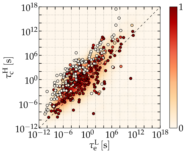
Fig. 1: Capture and emission time constants of oxide defects calculated with the NMP four-state model (circles). The density in the background shows the corresponding CET map.
