
 |
|
Biography
Prateek Sharma was born in Kota (Rajasthan), India. He recieved degree of Master of Science in electrical engineer from Linköping University, Sweden in 2012, where he was also invovled in smart dust and body area networks research projects. He joined the Institute of Microelectronics in March 2013 where he is working on the realiability systems in microelectronics.
Modeling Carrier Energy Distribution Function For Power Devices
Hot-Carrier Degradation (HCD) is sensitive to the high energy fraction of the carrier ensemble. Mathematically this means that HCD is determined by the high energy tails of the carrier Energy Distribution Function (EDF). Therefore, resolving these high energy tails is of special importance in the context of HCD modeling. Ideally, a proper carrier transport treatment has to be performed by a thorough solution of the Boltzmann Transport Equation (BTE). Since in bipolar devices both electrons and holes can contribute to HCD, the BTE needs to be coupled with the Poisson's equation. Solving these equations can be performed stochastically by a Monte-Carlo method or deterministically by expansion of the solution into a series of spherical harmonics. Both methods are rather complex and computationally demanding. The situation becomes even more complicated if the carrier transport treatment is aimed for a high-voltage device, e.g., a Laterally Diffused Metal-Oxide-Semiconductor (LDMOS) transistor.
Instead, a simplified carrier transport treatment based on post-processing of the results obtained using drift-diffusion and/or hydrodynamic schemes appears very attractive. The EDFs are then modeled as heated Maxwellian distributions. These EDFs are linked to the local electric field in the drift-diffusion based approach and to the carrier dynamic temperature if the hydrodynamic scheme is applied. Corresponding fitting parameters of such EDFs are found using information of moments of the BTE, such as the local carrier concentration. If we aim at further increasing the computational efficiency, electron temperature can be evaluated analytically from the electric field, which can be obtained from the drift-diffusion simulations.
Fig. 1 depicts an n-LDMOS with a length of 5um. Such a length makes this device very tough for Monte-Carlo simulations. The device was stressed at the drain voltage of 20V and the gate voltage of 2V. This drain voltage is quite high, therefore, proper simulation under these conditions using the deterministic BTE solver ViennaSHE is challenging. Fig. 2 demonstrates the carrier EDFs calculated with our method based on the drift-diffusion scheme and plotted in the key segments of the device, namely, at the source, bird's beak and the drain. These EDFs are compared to the ones obtained from the ViennaSHE simulations performed on this device. It is worth to emphasize that this comparison is performed only for the model calibration, while for real HCD simulation our simplified approach is expected to be used.
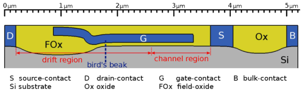
Fig. 1: The schematic representation of an n-LDMOS.
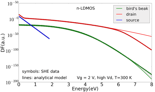
Fig. 2: The carrier distribution functions simulated using the drift-diffusion based approach are calculated in four different positions in n-LDMOS, namely, drain, source, bird's beak and the drift region. One can see that these DFS are severely non-uniform and demonstrate pronounced high-energy tails.
