
 |
|
Biography
Viktor Sverdlov received his MSc and PhD degrees in physics from the State University of St.Petersburg, Russia, in 1985 and 1989, respectively. From 1989 to 1999 he worked as a staff research scientist at the V.A.Fock Institute of Physics, St.Petersburg State University. During this time, he visited ICTP (Italy, 1993), the University of Geneva (Switzerland, 1993-1994), the University of Oulu (Finland,1995), the Helsinki University of Technology (Finland, 1996, 1998), the Free University of Berlin (Germany, 1997), and NORDITA (Denmark, 1998). In 1999, he became a staff research scientist at the State University of New York at Stony Brook. He joined the Institute for Microelectronics at the Technische Universität Wien, in 2004. In May 2011 he received the venia docendi in microelectronics. His scientific interests include device simulations, computational physics, solid-state physics, and nanoelectronics.
Modeling Silicon Spintronic Devices
The breathtaking increase in performance and speed of integrated circuits was made possible by continuous miniaturization of Complementary Metal-Oxide-Semiconductor (CMOS) devices. On this exciting path numerous outstanding technological challenges have been resolved. However, growing technological challenges and soaring costs are gradually bringing CMOS scaling to an end and thus putting ponderable constrains on future computational performance improvement. Therefore, a search for alternative technologies and computational principles is accelerating. As the electron charge, the spin of an electron is considered for future logic and memory device applications. It is characterized by two projections — up or down — and it can change its orientation rapidly by consuming an amazingly small amount of energy. Silicon routinely used by the semiconductor industry is very attractive for future spin-driven applications. Electrical spin injection into a silicon wafer, spin propagation and detection were already demonstrated at room temperatures. However, spin fundamental relaxation mechanisms in silicon-on-insulator structures promising for Metal-Oxide-Semiconductor Field-Effect Transistors (MOSFETs) beyond 14nm node are not well understood and require urgent attention.
We find the spin wave functions and spin relaxation matrix elements by employing the corresponding low-energy effective Hamiltonian with the electron spin included. The wave functions in the two [001] valleys - two spin projections basis contain four components. The large components correspond to the envelope quantization functions located near the corresponding valley minimum described by the face factor. The smaller components depend on the strength of the effective spin-orbit interaction linearly. When tensile stress along [110] direction is applied, the amplitude of those components responsible for spin relaxation is greatly reduced, indicating that stress can also be used to inhibit spin relaxation (Fig. 1).
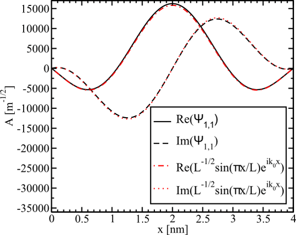
Fig. 1: The wave function components responsible for spin relaxation are reduced by tensile shear strain.
