
 |
|
Biography
Stanislav Tyaginov was born in Leningrad (now Saint-Petersburg) in 1978. He received his MSc degree in physics (specialization: the physics of semiconductors) in 2002 and his doctoral degree in physics in 2006 (his PhD was devoted to the problem of the impact of insulator thickness non-uniformities on MOS tunnel structure characteristics). He joined the Institute for Microelectronics in January 2008 as a post-doc researcher. His scientific interests include the modeling of HCI-related degradation and TDDB as well as tunneling phenomena in MOS devices.
Physical Modeling of Hot-Carrier Degradation for Short- and Long-Channel MOSFETs
Hot-Carrier Degradation (HCD) is a highly complex phenomenon involving a wide hierarchy of physical effects. This hierarchy connects the microscopic level of defect generation with the device physics level. HCD is widely accepted to be due to the dissociation of passivated Si-H bonds at or near the dielectric/semiconductor interface. This dissociation is induced by the charge carriers in the channel which interact with the bonds. The efficiency of such an interaction is defined by energies deposited at the interface by carriers from the ensemble moving through the device. Therefore, the crucial link in the aforementioned hierarchy between the device and microscopic levels is the carrier transport treatment, which is essential for a proper capture of bond-breakage kinetics as well as for modeling of the degraded transistors. Thus, an adequate description of carrier transport based on a thorough solution of the Boltzmann Transport Equation (BTE) is expected to be the central aspect of any physics-based hot-carrier degradation model. The complexity of this detrimental phenomenon results in a few issues related to its understanding and modeling. If the high-energetical fraction of the carrier ensemble is substantially populated, a bond dissociation event can be triggered by a solitary hot carrier via excitation of one of the bonding electrons to an AntiBonding (AB) state, the AB-process. These hot carriers are unlikely to be found under low stress/operating voltages. Instead, a series of colder carries can induce the Multiple Vibrational Excitation (MVE) of the bond followed by its rupture. In previous attempts of HCD modeling, these mechanisms were considered to be independent. This is, however, not physically reasonable because they are just competing pathways of the same bond-breakage reaction and need to be modeled consistently.
Another important question related to HCD is the role of Electron-Electron Scattering (EES). In this context, there are contradictive claims: (i) EES plays the dominant role in HCD observed in Metal-Oxide-Semiconductor Field-Effect Transistors (MOSFETs) of the 180nm node and beyond vs. (ii) the idea that the role of EES is dramatically overestimated. Furthermore, although the role of the bond-breakage energy dispersion has been repeatedly discussed in the literature, this information has not yet been incorporated into any physics-based HCD model. The same is also relevant for the energy lowering due to the interaction of the bond dipole moment with the oxide electric field.
We have developed and verified a physical HCD model which is implemented into the deterministic BTE solver ViennaSHE. The model consistently considers the AB- and MVE-mechanisms as well as all their possible combinations when the bond is excited to an intermediate level (with a lower potential barrier for hydrogen release) by the MVE-mechanism and then broken by the AB-process. The fast and flexible simulator ViennaSHE allows for the incorporating of EES into the carrier transport treatment. The activation energy dispersion and its lowering due to the field-dipole interaction are also consolidated into the simulation framework.
To validate the model, we used two types of SiON nMOSFETs with gate lengths of 65nm and 150nm. The devices were stressed at their HCD worst-case conditions. The model was verified in order to represent the linear drain current change vs. time in both devices (see Fig. 1 and 2) stressed under different conditions and using the same set of model parameters. Fig. 1 and 2 depict theoretical and experimental changes of the linear drain current as a function of time as well as characteristics computed neglecting one of the model ingredients (shown for the 65nm and 150nm devices, respectively). First, one can see that the AB-process plays a crucial role. The effect of EES is especially prominent in the 65nm device, becoming less pronounced in the 150nm counterpart. Relative contributions of the MVE-process and the field-dipole interactions increase with time, while neglecting the dissociation energy dispersion leads to underestimated HCD. Overall, the model is in excellent agreement with the experiment.
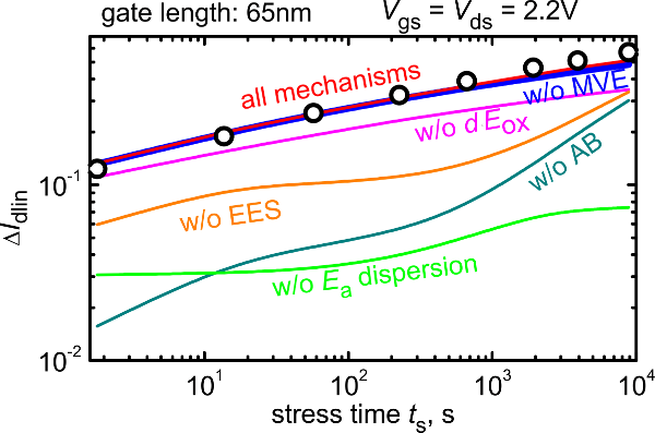
Fig. 1: The relative linear drain current change (normalized to the current in the fresh device) as a function of time for the 65nm device stressed at gate and drain voltages of 2.2V: experiment vs. theory. To check the role of different model ingredients we also have plotted degradation curves obtained neglecting one of these ingredients.
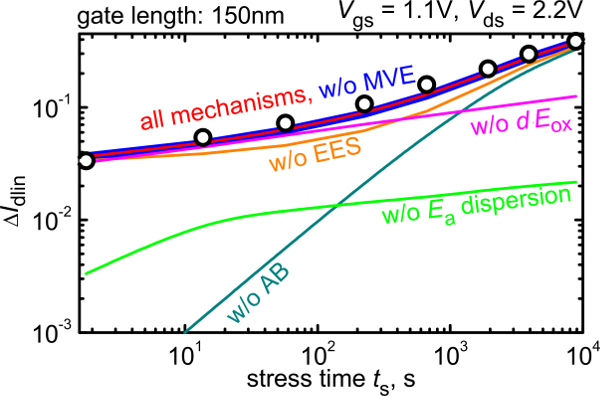
Fig. 2: The same as in Fig. 1 but for the 150nm counterpart which has been stressed at a gate voltage of 1.1V and a drain voltage of 2.2V.
