 |
|
Biography
Al-Moatasem El-Sayed was born in Sheffield, United Kingdom in 1988. He completed his Masters in chemistry at the University of Manchester in 2010. He went on to do his Ph.D in physics at University College, London, focussing on atomistic modeling of point defects in oxides. He then joined the Institute of Microelectronics in June 2015, his current research interests are modeling of point defects in oxides and their effect on electronic devices.
The Effect of Electric Fields on Point Defects
Our work is focused on understanding electronic devices at an atomic level. This is accomplished using simulations ranging from first principles quantum mechanical calculations to classical simulations. Our goal is to study reliability and breakdown in devices. This research encapsulates a number of devices, such as field-effect transistors and resistive switching memory. Improving these devices involves addressing reliability issues and understanding the fundamental mechanisms of resistive switching. We aim to understand these mechanisms using state-of-the-art atomistic modeling tools. In particular, my research involves using density functional theory implemented through highly parallelized codes, which have been widely used to identify and develop models of point defects in oxides.
Over the past couple of years, we have been particularly focused on how electric fields affect defect processes in oxides. Dielectric layers composed of metal oxides are routinely subjected to external electric fields during the course of the normal operation of electronic devices. The calculation of defect properties in oxides is generally made under zero field conditions. As mentioned previously, however, electronic devices experience rather high applied electric fields during operation. Previous atomistic calculations of defects used in the study of electronic reliability issues have included electric fields as an empirical parameter, with models subsequently built upon these calculations. In fact, many of these phenomenological theories suggest that electric fields strongly affect the properties and mobility of defects in oxide films and can even facilitate the creation of new defects. Our recent calculations have therefore explicitly included an electric field within our ab initio calculations using the Berry phase method.
We have shown that an applied field negligibly affects the barrier to creation of new defects in various materials. For example, Fig. 1 shows the barrier to breaking an Si-O bond in SiO2. The red lines indicate the energy profile up to a field of 10 MV cm-1, close to the breakdown field of SiO2. One can clearly see that such a high electric field barely changes the reaction profile. Furthermore, our research implicates intrinsic electron traps in a number of processes. In particular, electron injection plays an important role in the generation of new defects and can directly lead to breakdown.
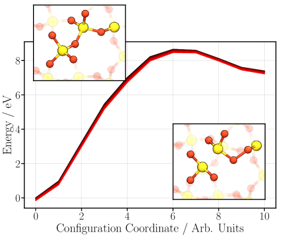
Fig. 1: The energy profile associated with breaking an Si-O bond and forming a defect in α-quartz. The x-axis represents the configuration coordinate of the defect generation, while the y-axis shows the system's total energy. The left and right insets show the atomic structures of the initial and final configurations, respectively. Multiple lines are shown in this plot. The redder lines, which are always lower in energy, are those for which a field of up to 10 MV cm-1 was applied.