 |
|
Biography
Xaver Klemenschits was born in Vienna in 1994. He studied Nanoscale Physics at the University of Birmingham, England, for which received the degree of MSci in 2017. He joined the Institute for Microelectronics in August 2017, where he is working on topography simulation using different deposition and etching models.
A Unified Feature Scale Model for Etching in SF6 and Cl Plasma Chemistries
Miniaturization has been the driving force behind the rapid growth of the technology industry for several decades. As microelectronic device dimensions have been decreasing, increasingly challenging lithography and fabrication limitations have been overcome. Complex production techniques have been developed to meet the dimensional requirements given in the "International Technology Roadmap to Semiconductors".
Transistor high-k gate stack patterning is currently one of the greatest challenges in advanced-node semiconductor fabrication. The complex, layered gates incorporate several materials, such as silicon, titanium, hafnium and silicon dioxide, all of which require a carefully controlled etching sequence. Even a single layer in a gate may require multiple etch steps, involving different chemistries, in order to achieve fine control over the details of the resulting geometry, such as sidewall tapering. Many of these etch steps include the simultaneous deposition of polymers on the sidewalls and ion-enhanced directional etching elsewhere, to achieve straight etch profiles. These polymers form a passivation layer, which will protect the underlying material in subsequent etch steps, preserving the tapered sidewalls. In order to optimise the simulation of these complex processes used in modern gate stack patterning, a unified feature scale model tunable to the individual steps is crucial.
Such a model was implemented in ViennaTS, a topography simulation tool employing level-set representations of surfaces, thereby enabling the unified simulation of intricate microelectronic process flows. As can be seen in Figure 1, different materials can be modeled independently and accurately in order to understand the interactions between them, which is especially important for characterizing the behavior of thin passivation layers, their effect on subsequent etch steps and thus the final geometry. The simulation depicted shows the most important etch steps in the 14FDSOI process of the 14 nanometer node and the resulting geometry.
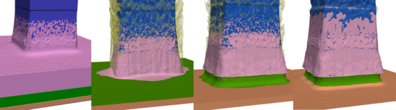
Fig. 1: The full etching flow of different materials in the gate stack in the 14FDSOI process. The gate geometry is shown after: (a) Poly-Si (pink) Main Etch in SF6 plasma with resulting passivation layer (blue); (b) Poly-Si Over Etch in HBr plasma with additional passivation layer (yellow); (c) TiN (green) Main and Over Etch in Cl2 plasma; and (d) HfO2 (orange) Wet Etch.