 |
|
Biography
Theresia Knobloch was born in Vienna in 1992. She received her BSc degree in Technical Physics and the degree of Diplomingenieur in Microelectronics from the Technische Universität Wien in 2014 and 2016, respectively. She joined the Institute for Microelectronics in April 2016, where she is currently working on her doctoral degree. Her current research topic are novel devices based on two-dimensional materials.
The Role of Contacts in MoS2 Field-Effect Transistors
Over the past decades, transistor scaling has followed Moore’s Law, assuring higher package densities, faster switching speeds and reduced power consumption. Today, conventional silicon technology is gradually approaching the scaling limit, however, with gate lengths of only a few nanometers, where parasitic short-channel effects strongly degrade device performance. One way of suppressing short channel effects would be through the usage of new channel materials like, for example, 2D semiconductors, which show excellent electrostatics due to their ultimate thinness. Out of the large group of 2D materials, Molybdenum Disulfide (MoS2) offers very promising properties, among them a large band gap, moderate mobilities and heavy effective carrier masses.
Even if the cross section of a metal-oxide-semiconductor field-effect transistor (MOSFET) using MoS2 as a channel material (see Fig. 1a) bears similarities to the cross section of a planar silicon device (see Fig. 1b), the operation principle is substantially different. The silicon device is turned on by the formation of an inversion layer below the oxide, whereas the MoS2 device is in the on-state if the applied potential suffices to deflect the band edges to such an extent that a large tunneling current can flow through the Schottky barriers at source and drain. Thus, in silicon devices, the on-current consists of minority carriers of the p-doped channel, for example, rendering the device in Fig. 1b) an n-type MOSFET. MoS2 devices, on the other hand, are in principle ambipolar, meaning that both electrons and holes can dominate the current flow. However, intrinsic defects in the MoS2 cause a native n-doping, and the work functions of the metals used for contacting MoS2 are aligned close to the conduction band edge, thereby enhancing the electron flow. Thus, MoS2 transistors usually show n-type behavior. In short, while the pn-diodes in the silicon channel control the current flow in a silicon device, the Schottky diodes at the contacts control the current flow in MoS2 transistors.
While in conventional devices Schottky barriers at the contacts are suppressed by extensive doping of the semiconductor at the metal boundary, this is no longer true for 2D-based devices. In order to accurately describe the characteristics of 2D-based MOSFETs, we therefore extended our drift-diffusion based TCAD model to correctly account for Schottky barriers using the models suggested by Appenzeller et al. As the ohmic approximation with a fixed Fermi level no longer holds(see Fig. 2a), we use a Schottky contact model (Fig. 2b), where both the thermionic contribution of electrons flowing over the barrier and the field contribution of electrons tunneling through the barrier are taken into account.
In Fig. 3a), the different contributions to the current in our model are shown, and the modeling results are compared to measured characteristics. It is clearly visible that the tunneling current dominates over the thermionic emission current in the on-state. This is because the decay length of the potential at the source/drain contacts is very short due ultimately to the thin 2D channel. This causes a small Schottky barrier width and hence large tunneling currents. In Fig. 3b), the impact of different metal work functions on the current is illustrated, illustrating that the current decreases by several orders of magnitude for an increase of the Schottky barrier height.
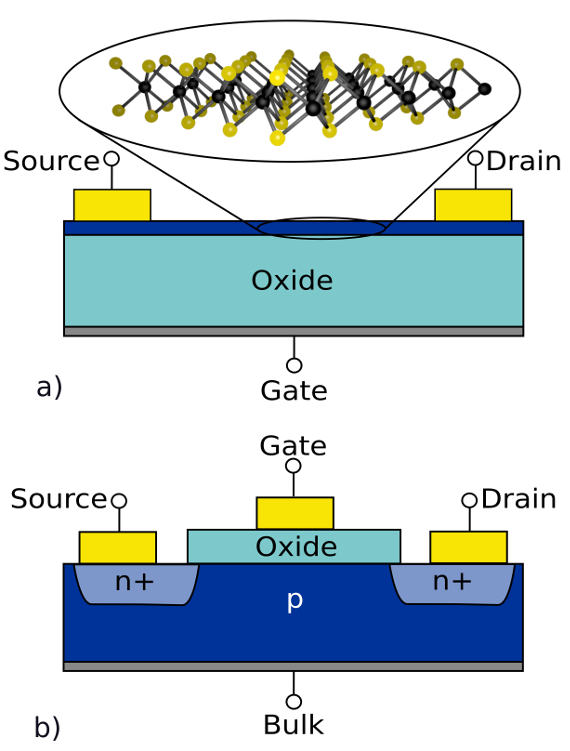
Fig. 1: Comparison of the cross sections through a back-gated MoS2 MOSFET (a) and through a planar silicon MOSFET (b). In addition, in Fig. 1a), the atomic structure of a MoS2 monolayer is shown. Here, the yellow spheres depict sulfur atoms and the black spheres molybdenum atoms.
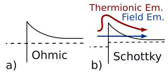
Fig. 2: Schematic showing the band bending at a metal/semiconductor contact. The solid line represents the band edge of the semiconductor and the dashed line the location of the Fermi level.
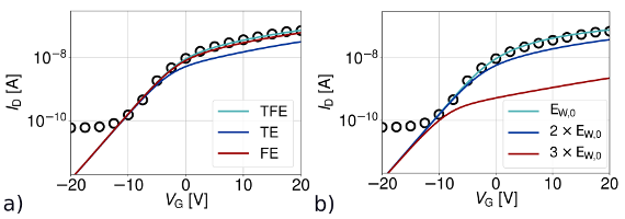
Fig. 3: The circles are measurement points and the solid lines simulation results. In Fig. 3a), the different contributions to the current over the Schottky barrier are shown. In Fig. 3b), the impact of different metal work functions, effectively changing the Schottky barrier height, is demonstrated.