|
|
Biography
Alexander Makarov was born in Volgograd, Russia, in 1985. He studied information technology at the Volgograd State Technical University, where he received the BSc degree in 2006 and MSc degree in 2008. He joined the Institute for Microelectronics in October 2009 and has obtained the doctoral degree in March 2014. He is currently employed as a post-doc researcher. His scientific interests include Monte-Carlo simulations and nonvolatile memory device modeling.
Physics-Based Modeling of Hot-Carrier Degradation in FinFETs
Properly tackling reliability issues is required for the introduction and optimization of novel transistor nodes. Although the problem of device reliability includes a number of concomitant phenomena, for the most recent transistor topology - the FinFET architecture - hot-carrier degradation (HCD) has been reported as the most detrimental one. Whilst HCD in FinFETs has been the subject of extensive experimental research and modeling in recent years, a detailed understanding of HCD in these devices is still lacking. For instance, substantial experimental effort has been devoted to the problem of the exact device geometry optimization required to suppress HCD. In this context, consensus on the optimal fin width needed to alleviate HCD has not been reached. Our main task was therefore to analyze the peculiarities of HCD in FinFETs. We paid special attention to the localization of hot-carrier damage. We also studied the interface state density (Nit) throughout the fin/dielectric interface.
To achieve this goal, we used our physical model for HCD, which was validated to represent the linear drain current degradation in FinFETs (Fig. 1a). It is important to emphasize that in order to model HCD in FinFETs, we employed a very similar set of model parameters as for HCD simulations in planar MOSFETs and high-voltage devices. For the first time, we calculated the distribution of the trap density over the fin/dielectric interface (Fig. 1b) and revealed the location of the most damaged spot (in the upper corner of the fin's drain side).
To investigate the effect of geometrical parameters on HCD in FinFETs, we used three series of virtually fabricated FinFETs with an identical architecture but with varying gate lengths, fin widths and fin heights. The model was applied to investigate the effect of these geometrical parameters on HCD. We demonstrated that HCD becomes more severe in shorter transistors. This result appears to be quite natural and consistent with previous findings. Device characteristics change less in FinFETs with narrower fins, while the fin height influences HCD behavior insignificantly. Finally, we showed that a thorough extraction of device lifetime is possible only by using a physics-based model for HCD. Consequently, simplified empirical approaches have very limited applicability.
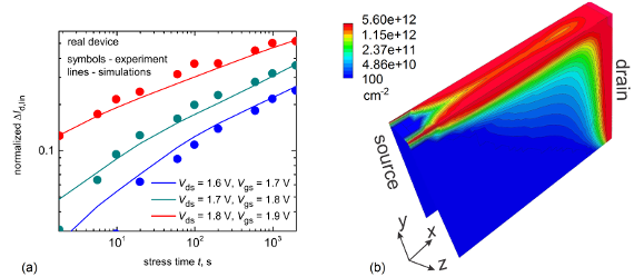
Fig. 1: (a) Measured and simulated ΔId,lin(t) traces for three stress conditions show very good agreement. (b) The Nit density present throughout the fin/dielectric interface of the device.