 |
|
Biography
Michael Waltl was born in Oberndorf near Salzburg, Austria. He received the BSc degree in electrical engineering, the degree of Diplomingenieur in microelectronics, and the doctoral degree in technical sciences from TU Wien in 2009, 2011, and 2016, respectively. His scientific focus is on experimental characterization and modeling of reliability issues prevalent in semiconductor devices and devices with more exotic 2D materials. In this field, he primarily studies bias temperature instabilities in modern transistors. He also leads the device characterization laboratory at the institute, where he is in charge of developing electrical measurement methods.
Improved Measurement Set-Up for Silicon-Carbide MOS Transistor Defect Spectroscopy
Although the fabrication processes of advanced transistors are continuously being improved, there are still a significant number of process-induced, electrically active defects in state-of-the-art MOS transistors. Through repeated charging and discharging, these defects cause a drift in the device threshold voltage, thereby significantly affecting the stable and reliable operation of the transistors. The number of defects is primarily determined by the materials used for the gate stack (SiO2, SiON or high-k materials), their thickness and the device geometry (i.e. the gate area). While advanced high-performance transistors are continuously scaled down to nanometer dimensions, silicon carbide (SiC) transistors, which are used for high-power applications, typically exhibit a gate length and gate width of several hundred micrometers. Due to this difference in scale, SiC MOS transistors contain a significant number of defects compared to advanced technology nodes.
As previously mentioned, by becoming repeatedly charged and discharged, the defects can significantly alter device characteristics, even when operating far below their nominal operating conditions. The impact of the defects themselves manifests as a drift in the threshold voltage, a change in the sub-threshold slope and a reduction in carrier mobility. To measure the defects' impact on device behavior, a dedicated defect measurement framework (TMI) has recently been designed and successfully used to study (single) charge trapping in (nanoscale) MOS transistors. To probe SiC power MOS transistors, the TMI has recently been extended by an ultra-low noise pattern generator with an output voltage of up to 48 V and a time resolution of 10 us. The high output voltage range is required as SiC power devices exhibit thick oxides. Furthermore, the ability to supply the pattern generator with battery power is highly beneficial for reducing the noise level, especially when currents in the sub-picoampere range must be measured at sampling rates of up to 100 kHz. With the extended bias ranges, defect-probing investigations into SiC MOS transistors can be performed.
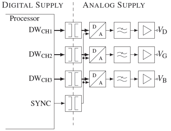
Fig. 1: Block diagram of the voltage pattern generator with the extended bias range required to probe MOS transistors with thick oxides.