 |
|
Biography
Yury Illarionov was born in Leningrad (now Saint-Petersburg) in 1988. He studied solid state physics at the Physical Science and Technology Faculty of St. Petersburg State Polytechnical University where he received the B.Sc. and M.Sc. degrees in 2009 and 2011, respectively. From 2010 to 2012 he studied advanced material science in Grenoble Institute of Technology (France) and University of Augsburg (Germany) in frameworks of Functionalized Advanced Materials and Engineering (FAME) Erasmus Mundus program and in September 2012 received a double European M.Sc. degree. His scientific carrier has started in October 2007 in Ioffe Physical-Technical Institute (Russia) and in November 2011 he joined the PhD program there. He also visited IRCELYON (France, May-July 2011) and Singapore Institute of Manufacturing Technology (Singapore, February-July 2012) as a young guest researcher. He joined the Institute for Microelectronics in February 2013. In January 2015 he received the PhD degree in semiconductor physics from Ioffe Physical-Technical Institute and in December 2015 the Dr.techn. degree from TU Wien. Since January 2016 Dr. Yury Illarionov is a postdoc researcher working on reliability of the next-generation 2D FETs with graphene, MoS2 and phosphorene.
Bilayer MoS2 Field-Effect Transistors with 2 nm Thick Crystalline CaF2 Insulators
Two-dimensional (2D) semiconductors are potentially suitable to help overcome the limitations of Si technologies by enabling More-Than-Moore FETs with channel dimensions in the few nanometers. This target cannot be realized without gate insulators scalable down to equivalent oxide thicknesses (EOTs) of below 1 nm, however, which would simultaneously maintain low gate leakages and high-quality interfaces with 2D channels. Unfortunately, the insulators currently used in 2D FET prototypes are still several tens of nanometers thick and do not satisfy the stringent scaling requirements. For instance, oxides known from Si technologies (e.g. SiO2, Al2O3 and HfO2) are amorphous when grown in thin layers, and hBN has unfavorable dielectric parameters and unfortunate band offsets to most 2D semiconductors.
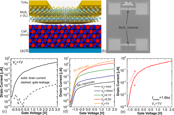
We have recently attempted to overcome this bottleneck by using epitaxial fluorite (CaF2) as an insulator in MoS2 FETs. CaF2 is a crystalline insulator with a wide bandgap (12.1 eV) and a relatively high permittivity (8.43), which makes the tunnel leakages through this material comparable to those through currently used high-k oxides. Furthermore, the F-terminated CaF2(111) surface is inert and does not produce any dangling bonds, thus leading to a well-defined quasi van der Waals interface with 2D materials (Fig. 1a). By transferring bilayer MoS2 films grown by chemical vapor deposition onto Si(111)/CaF2 substrates, we have fabricated hundreds of functional MoS2 FETs (Fig. 1b) with record-small gate insulator thicknesses of only about 2 nm (EOT about 0.9 nm).
In the first bare channel prototypes, we already achieved ultra-low leakage currents (Fig. 1c), on/off current ratios of up to 107 and subthreshold swings down to 90 mV/dec (Fig. 1d). At the same time, we found that our devices exhibit almost no hysteresis (Fig.1e). This is likely due to the small number of defects in crystalline CaF2 layers and the virtually defect-free MoS2/CaF2 interface. Through these studies, we have extended the natural stacking properties of 2D materials towards quasi van der Waals heterostructures with epitaxial fluorides. Our results present a route towards fully scalable 2D electronics, which is particularly promising given recent reports on epitaxial growth of 2D semiconductors on CaF2(111) crystals.

Fig. 1: (a) Schematic layout of our device with a quasi van der Waals CaF2/MoS2 interface. (b) Scanning electron microscope image of two devices. (c) Measured drain current and gate leakage. (d) Typical set of gate transfer characteristics at different drain voltages. (e) The gate transfer characteristics exhibit almost no hysteresis, even for kilosecond sweep times.


