

Next: 2.3 Limitations of the Barrier Material
AlGaAs Up: 2 The Principles of a HEMT
Previous: 2.1 Limitations of the Channel Material
InGaAs
2.2 Electron Energy Levels in
Strained Quantum Wells
When InGaAs is grown pseudomorphically on GaAs the InGaAs layer is
biaxially compressively strained because the lattice constant of unstrained
InGaAs is larger than that of GaAs. Compressive strain causes an increase
in Eg which acts contrary to the reduction in Eg
with increasing In mole fraction, i. e. the reduction of Eg
is partially canceled by the strain effect. The strained band gap energy  can be calculated by [19]:
 |
(4)
|
where the hydrostatic part DEh
of the energy shift reads
 |
(5)
|
and the uniaxial contribution DEs
of the energy shift reads
 . . |
(6)
|
 is
given by (2).
The values of the lattice constants a, the deformation potentials
d1 and d2 as well as the elastic constants
C11 and C12 for GaAs and InAs, respectively,
can be found in Table
2.1. The values for InxGa1-xAs are obtained
by linear interpolation between the numbers for the binary materials.
Due to the uniaxial strain the degeneracy of the valence band is canceled.
The positive sign in (6) holds for the shift
of the heavy hole band and the negative sign for the shift of the light
hole band. The investigations on strain dependence of the band discontinuities
in the literature are contradictory [20,
21, 22].
Because no consistent results could be found in the literature 60 % of
the energy difference between the conduction band and 40 % difference in
the heavy hole valence band is assumed for DEC
and DEV between GaAs and InGaAs
as well as for the heterojunction between AlGaAs and InGaAs as described
in Section 2.1.
In a quantum well the continuous energy levels of the conduction band
split up into discrete levels. The energy levels Ee can
be calculated by solving the Schrödinger equation for a single potential
well with finite barrier height. The symmetrical part of the solution is
given by
 |
(7)
|
which reveals the lowest energy Ee, i. e. the ground
state of the quantum levels in the potential well. In (7)
dC is the thickness of the quantum well, and h
is the Planck constant, and mAlGaAs and mInGaAs
are the effective masses of the barrier and channel materials, respectively.
For the current transport over a potential barrier the difference between
the energy level of the electron and the energy maximum of the barrier
has to be taken into account. Within MINIMOSNT only properties of
bulk material are used for the simulation models in the channel. To account
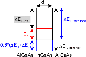
for strain and quantum effects an effective band gap Eg eff
and therefore an effective conduction band offset DEC
eff as shown in Figure
2.6 is calculated separately according to (4)
and (7) and used for the channel
material.
 Figure 2.6 Schematic conduction band diagram of an
InGaAs quantum well with AlGaAs barriers. For the energy difference of
an electron to surmount the barrier the change in Eg
due to strain as well as the quantum levels of electrons in the channel
have to be taken into account.
The unstrained conduction band offset DEC
unstrained is reduced by the bandgap shift due to strain and
the quantization of the electrons in the channel. Due to the critical thickness
a trade off between the In content x and the channel thickness dC
cr(x) has to be made as described in Section
2.1. Therefore the following considerations are based on InxGa1xAs
layers and the critical layer thickness corresponding to the In content
x. Given this limit for the thickness dC cr of a quantum
well for each In content the quantum level of electrons Ee
can be calculated "along" the critical thickness dC cr.
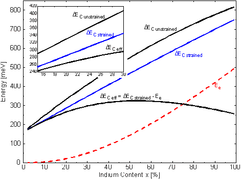
In Figure
2.7 Ee is shown for an Al0.2Ga0.8As/InxGa1-xAs/Al0.2Ga0.8As
quantum well versus the Indium content. Also DEC
strained and DEC unstrained
are shown. For a strained Al0.2Ga0.8As/In0.2Ga0.8As/Al0.2Ga0.8As
channel with a critical thickness of 14 nm the energy level of electrons
is 20.5 meV above the band edge (Ee= 26.5 meV for a 12
nm thick channel which is typically used). The shift in Eg
due to strain (DEh + DEs)
accounts for 45.5 meV. According to Figure
2.6 both effects reduce the unstrained DEC
from 331 meV to 265 meV. Figure
2.7 shows that DEC eff
could be increased to about 320 meV for an In content of more than 50 %.
But problems in epitaxial growth and effects such as surface roughness
and alloy scattering severely degrade the crystal quality and thus the
transport properties [23,
24,
25, 26].
 Figure 2.7 Conduction band offset of an unstrained
and strained Al0.2Ga0.8As/InxGa1xAs/Al0.2Ga0.8As
quantum well. Electron quantum level for the quantum wells along the critical
thickness (dashed line). Effective conduction band offset DEC
eff according to Figure2.6 (bold line).
Several attempts have been made to overcome the tight limitations of
pseudomorphic growth on GaAs substrates. One possibility is to change the
lattice constant for the growth conditions of the HEMT layers. This can
be achieved by growing thick relaxed InGaAs layers on the GaAs substrate
which is called metamorphic growth [27,
28,
29]
or by using InP as substrate. Figure
2.2 reveal the ternary systems InGaAs and InAlAs lattice matched to
InP. The two materials yield an DEC
of about 700 meV. In addition the electron velocity is substantially increased
compared to pseudomorphic InGaAs on GaAs as shown in Figure
2.4. For HEMTs on InP extrinsic fT's exceeding 300
GHz are reported [30].
The drawback concerning devices performance is low power capability. Due
to the small Eg in the channel breakdown occurs for relatively
low electric fields compared to GaAs based pseudomorphic HEMTs. But practically
the most severe drawback is the high cost of InP wafers, the small wafer
size (mostly 3'' today) and the incompatibility of the process technology
with other cheaper standard processes that are used for instance in a MESFET
production line.


Next: 2.3 Limitations of the Barrier Material
AlGaAs Up: 2 The Principles of a HEMT
Previous: 2.1 Limitations of the Channel Material
InGaAs
Helmut Brech
1998-03-11


 .
.

