Process TCAD
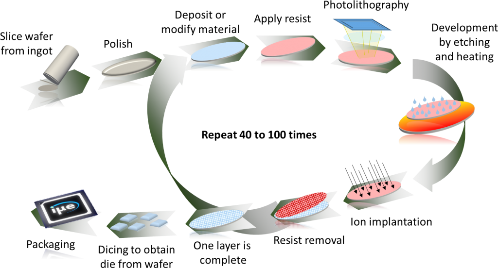
In order to understand how semiconductor devices are fabricated, we often rely on process technology computer aided design (TCAD) simulations. These types of simulations include a variety of models for topography motion during etching and deposition, material modification during ion implantation and annealing, or material growth during oxidation. To fabricate a complete integrated circuit (IC), these additions and modifications occur in several patterning cycles which include photolithography, as given in Fig. 1. Our research encompasses the modeling and simulation of a wide number of relevant processes using advanced simulation frameworks and high performance algorithms. Some of our achievements are described here.

Process Simulation Framework
Usually, it is very difficult to perform surface- and volume-related simulations within the same process TCAD framework. This is because volume-related models, such as oxidation, ion implantation, and diffusion, require a volume description of the geometry being modified, while surface-related simulations require the precise movement of a surface due to material deposition or etching. Each of these problems are ideally addressed quite differently. Surface motion is most often simulated without explicitly defining the location of the surface, but rather by storing surface location information on a Cartesian grid where all grid points contain a value representing the distance to the surface and performing advection by solving the Level Set equation. Volume problems require an explicit mesh which defines the geometry of the material being modified and all of its relevant parameters.
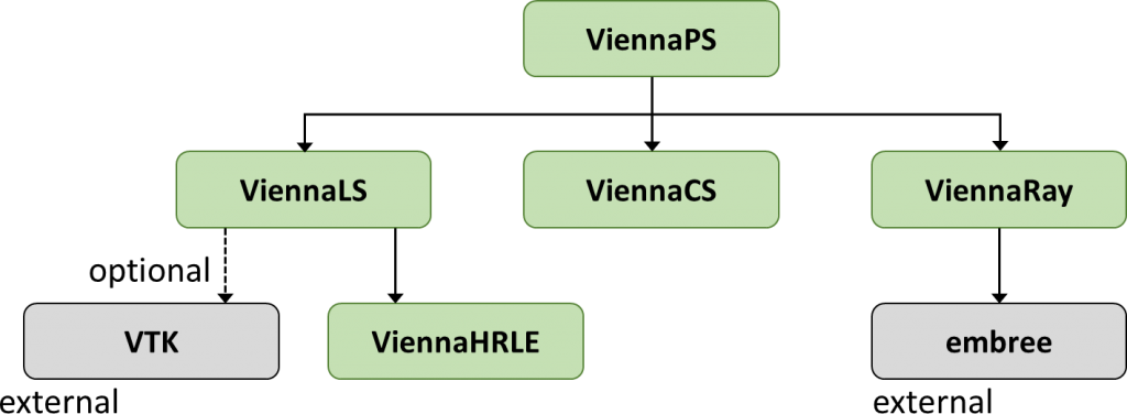
Very often, to perform a sequence of steps which includes a variation of surface and volume descriptions, the current state-of-the-art solution requires several frameworks and geometry conversions between implicit surface, explicit surface, and explicit volume representations. However, these conversions result in longer simulation times and they increase the potential for numerical errors and inaccuracies in the result. To address these concerns, in this project, the research will be focused on finding a solution which merges an implicit representation of the surface with local material information on the same grid and data structure. This will remove the need for computationally expensive and error prone conversions between implicit and explicit representations currently being applied. We will then investigate the application of this framework on physical models for highly relevant processes such as atomic layer deposition (ALD) and sputter etching, which are considerably dynamically governed by processes which have to be resolved on the atomic scale. The background to this research is our in-house process simulation framework, ViennaPS (see Fig. 2), which is able to natively treat both surface and volume problems. This is done by simultaneously storing the level set (LS) which defines the surface and a cell set (CS) which defines the volume, on the same data structure. When combined with ViennaRay, which provides the Monte Carlo Ray Tracing functionality, we can simulate a large set of topography and process steps during the formation of semiconductor devices within the same framework. This framework is ideally suited for the industry’s push towards design technology co-optimization (DTCO).

Multi-Scale Process Modeling
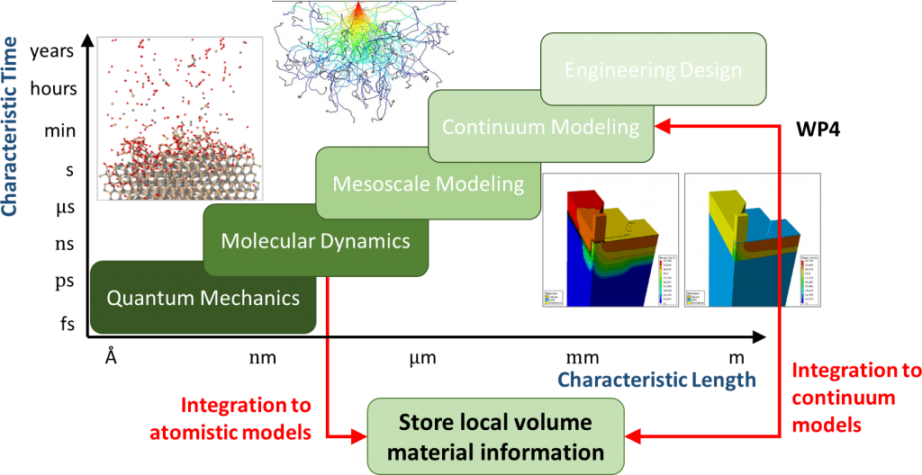
A multi-scale approach to simulation involves models at different time and size scales. Essentially, models which look at the molecular or atomistic level of a device or process can only be realistically simulated for very short times and with relatively few atoms (few thousand at the most). On the other hand, to perform process TCAD and to generate devices, continuum models are essential. However, many times, these continuum models are not physical, relying on empirical observations which do not contain the essential physics of the process therein. To include the basic physical knowledge in continuum models, a multi-scale approach needs to be applied, as shown in Fig 3. Device TCAD developers have already realized that a multi-scale approach to device simulation is essential, which is why the most advanced commercial tools provide an interface from ab-initio to compact modeling of advanced devices. This type of approach is also essential for process TCAD, which is what we will investigate in this project, together with our industry partner SILVACO.
The research in this project will be aimed at developing a combined molecular dynamics (MD) and level set (LS) framework to enable ab-initio predictive doping activation and motion especially following a variety of ion implantation conditions, in non-standard and not well characterized materials like for instance silicon carbide (SiC). SiC is a material which is likely to replace silicon in many high voltage and high temperature applications, due to its improved efficiency over silicon. We will then apply this multi-scale approach to investigate doping through diffusion in materials beyond silicon, such as germanium, which are likely to be used as the channel in post-silicon devices, beyond the 3nm technology node. This project will set the academic and industrial partner on the path to be at the forefront of process TCAD research since the integration of new materials in everyday devices is an inescapable reality.

Process Emulation
Process emulation is a relatively recent research direction, when it comes to process TCAD. The general concept is that, very often, physical models of topography motion during deposition and etching are not necessary in order to describe the final surface. Rather, an empirical model can be applied through process emulation. These types of models do not simulate a process in time; instead, they only emulate its outcome. Due to the nature of process emulation models, it is more straight-forward to implement them with explicit surfaces, since they allow for the movement (or drawing) of surfaces and interfaces over large distances, seeing that no time-stepping is required. However, explicit surfaces often require re-meshing and the discretization of the simulation space into voxels, making them undesirable for the emulation of many types of fabrication processes. Furthermore, they are not compatible with physical process simulations, in case that a user would like to perform physical simulation on one set of fabrication steps while emulating other steps. Therefore, we are working on a solution which can be applied over a broad range of geometric descriptions, including the Level Set, making it compatible for integration in a standard process TCAD framework.
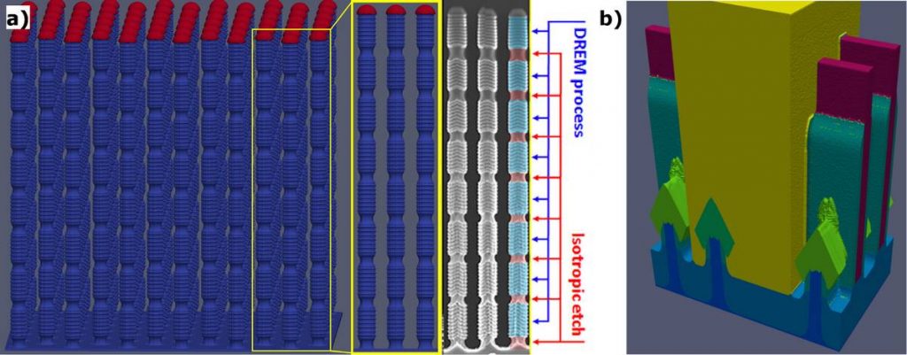
In our approach, we apply emulation with a method called Geometric Advection in order to differentiate it from Transient Advection techniques which involve time-stepping. As an example of the power of Geometric Advection, Fig. 4 (a) shows the emulation results of sausage-chain like structures which are fabricated using several modified deep reactive ion etching (DRIE) steps. To emulate these 80 cycles required less than 15 minutes on a standard desktop PC. Fig. 4 (b) shows an entire SRAM cell in the 5 nm FinFET technology node, which was performed using a combination of physical Monte Carlo based process models (fin patterning, spacer etching, and fin recess), transient topography models (epitaxial growth), and process emulation (shallow trench isolation deposition and etching, dummy gate deposition and patterning, spacer deposition, interlayer dielectric deposition and etching, dummy gate removal, and high-K metal gate deposition). The total time required to simulate the entire cell was less than 16 minutes, 88% of which was required for the physical models.

