 |
|
||||
BiographyLado Filipovic is an Assistant Professor (tenure-track) of Modeling and Simulation of Integrated Semiconductor Sensors at TU Wien. He obtained his venia docendi (habilitation) in Semiconductor Based Integrated Sensors and his doctoral degree (Dr.techn.) in Microelectronics from TU Wien in 2020 and 2012, respectively. He holds a Master’s degree in Applied Sciences (MASc.) from Carleton University in Ottawa, Canada, which he obtained in 2009. He has served as a reviewer for several DFG (DE) and EPSRC (UK) projects, has edited a book on Miniaturized Transistors, and has reviewed for many leading journals. He is a Senior Member of the IEEE and is an active member of the Technical Program Committee for outstanding IEEE sponsored conferences, such as IEEE Sensors, SISPAD, and IIRW. He has been a Principal Investigator in various research projects funded by, e.g., the EU FP7 and Horizon 2020 programs and the Austrian Research Promotion Agency (FFG). His primary research interest is studying the operation, stability, and reliability of novel semiconductor-based sensors using advanced process and device TCAD approaches. One of his research pillars is combining physical and empirical modeling approaches, specifically in process TCAD. With his team, he is actively investigating metal oxide semiconductors and two-dimensional materials, e.g., graphene, MoS2, and phosphorene for the detection of environmental pollutants and biomarkers from exhaled breath. |
|||||
Process Simulation for Design-technology Co-optimization
The simulation of semiconductor fabrication steps using process technology computer-aided design (TCAD) has become an integral component of novel device designs within the design-technology co-optimization (DTCO) cycle. While the fabrication of previous generations of semiconductor devices could be described using a set of typical processes and device structures, the recent trend in application-specific designs requires a broad examination of different geometries and materials. This means that all aspects and scales of research, from material to circuit, must be informed by one another. Knowing a single fabrication step's impact on the geometry of a desired device can further inform the circuit designer of its impact on circuit performance. This information can then be fed to the process engineer in order to calibrate and improve the process for improved circuit performance. However, doing all these feedback loops and cyclical DTCO steps using experiments alone results in time- and cost-intensive studies, making them largely unfeasible. Therefore, the integration of process simulations with device and circuit simulations is essential for the successful design of future semiconductor devices and technologies.
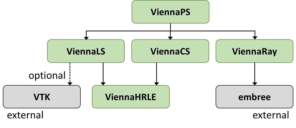
For DTCO, relying on purely physical simulations using Monte Carlo ray tracing is not ideal. These types of simulations require long run times and result in a geometry which can have significant numerical artifacts, such as an artificial surface roughness, making it difficult to provide a quality mesh of the final structure. A high quality mesh is required to import the device into a device simulator and to finally make the link between process and device TCAD. As an alternative, process emulation can be performed, whereby the geometrical features of a structure are drawn to represent the final device. However, linking physical process parameters with fast process emulation is difficult, since emulation inherently loses physicality due to not being solved in time. To overcome this, we are working on compact models which aim to provide a model suitable for emulation, based on highly physical simulations. This is enabled by an in-house designed process TCAD framework (ViennaPS), which includes a level set library (ViennaLS), a cell set library (ViennaCS), and a ray tracer (ViennaRay), as depicted in Fig. 1.
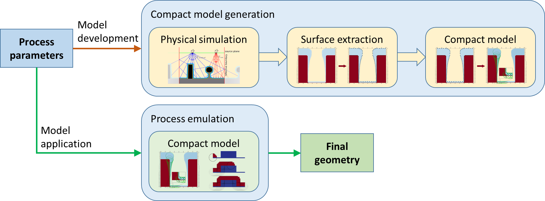
The process simulation framework ViennaPS provides the ability to implement both highly physical models and quick geometric models for process emulation — within the same framework — while using the level set to describe the surfaces in all cases. This capability was exploited previously in order to study large circuits, such as an SRAM cell, by using a combination of process emulation and simulation. The simulation was only used for the processing steps where absolutely required for the specific study. We are currently applying this framework in order to design compact models based on physical simulations for process emulation. Physical simulations using Monte Carlo ray tracing are applied in order to generate many structures, for which the surface is subsequently extracted and used to devise compact models. These compact models are then able to quickly generate the emulated geometrical features while still containing the physical information about specific process parameters. These two sequences are shown in Fig. 2, where the compact model is able to quickly replicate the resulting structure based on the applied process parameters and the initial geometry. The final geometry can then be implemented using approximate constant rates and time-discretized simulations, geometric advection, or using Boolean operations. A thorough set of compact models will allow the implementation of a quick solution to DTCO components which link process-related variations all the way to their impact on the final integrated circuit. We have tested this approach with a compact model for the highly reactive chemical vapor deposition in a rectangular trench, and have been able to achieve a simulation speedup of 100 times without any loss of accuracy.

Fig. 1: Dependencies of the ViennaPS process simulation library on other software libraries for core functionalities. Additional non-essential features are connected using dashed lines, while external libraries are filled with a grey background and labelled as external.

Fig. 2: Generation of a compact model from extracted surfaces which are generated using a physical Monte Carlo ray tracing approach. This sequence is enabled using in-house process simulator ViennaPS.


