 |
|
||||
BiographyYoanlys Hernández Barrios received the bachelor’s degree from Exact Sciences Pre-University Vocational Institute, Pinar del Río, Cuba. He studied Biomedical engineering at the “CUJAE” Technical University in La Habana, Cuba. In August 2015, he began his Master studies focusing on Solid State Electronics at the Center for Research and Advanced Studies of the National Polytechnic Institute (CINVESTAV-IPN) in Mexico City. In August 2020, Yoanlys finished his PhD studies at the same research center specializing in characterization, simulation, fabrication and modeling of thin film transistors and circuits based on amorphous metal oxides semiconductors. In March 2021 he joined the Institute for Microelectronics as post-doctoral researcher and will focus on semiconductor devices and circuits reliability. |
|||||
Impact of Bias Temperature Instability on the Performance of SiC-based MOSFETs for High Power Electronics
High Power MOSFETs designed using silicon carbide (SiC) are widely applied in devices for motor drives, solar inverters, and charging stations for electric vehicles. The complex electronic circuits employed in these systems are based on several basic topologies, and their robust operation is key for long-term operational stability. One of the most dominant topologies is the so-called DC-DC Boost converter. To ensure high power conversion efficiency of such circuits, a large carrier mobility, steep sub-threshold slope, and low ON-resistance (RDS(ON)) are essential requirements of the utilized transistors. However, the transistor performance is severely affected by time-zero and time-dependent variability issues which must be taken into account during circuit design.
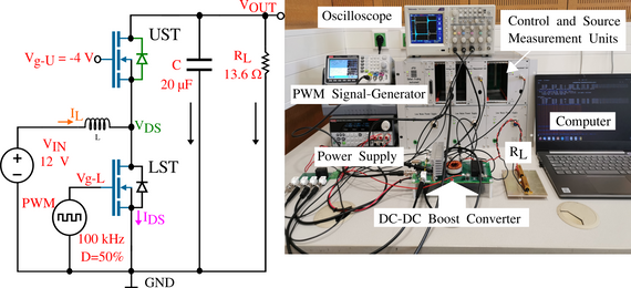
We use the experimental setup shown in Fig. 1 in this study. The device under test (DUT) is a commercially available SiC Power MOSFET C3M0075120K, provided by Wolfspeed (formerly Cree Inc.). Even though bias temperature instability (BTI) has a negligible effect on the total switching losses, it affects RDS(ON) as well as the static ON-state power loss (PON) of the MOSFETs. For this reason, to predict the real behavior of ΔVth over time, it is crucial to account for a physical trapping model. This way we can estimate the real PON during the ON-state operating time as accurately as possible. Our reliability study is divided into two steps: (i) We extract ΔVth using the physical charge trapping model implemented in our physical reliability simulator Comphy. In our work, we consider an extended DC long-term measure-stress-measure (MSM) scheme, where a constant stress bias of 25 V is applied to the gate contact of the transistor before the recovery phase is recorded. (ii) We make use of NGSPICE simulations to introduce the ΔVth variation within the SPICE model for the transistor, allowing to analyze the aging behavior of the DUTs at circuit scale. The device manufacturer provides the SPICE model of the non-aged DUT. Each ΔVth corresponds to a certain degree of degradation in time and is considered by adding a voltage source to the gate of the transistors.
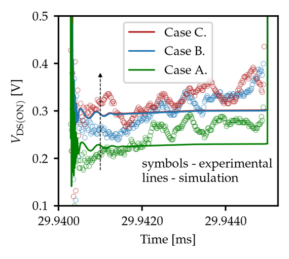
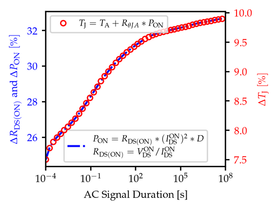
We analyze the BTI impact on the circuit performance under three different conditions: (A) non-degraded, (B) DUT is stressed for 10 ks, and (C) DUT is stressed for 20 ks. For all tested cases, we reproduce the observed behavior of the circuit in the simulations. During ON-state operation, an increase in RDS(ON) leads to a subsequent increase in PON. Using the extracted ΔVth values from Comphy, we reproduce by simulation the experimental circuit operation, see Fig. 2. With the tool-set calibrated, it is possible to estimate the aging behavior of the DUT over a long operating time, which is crucial to predict the system's lifetime. With the extracted ΔVth distribution from Comphy for an operating time of ten years, which is possible due to the thermal activation of charge trapping, we estimate the increase in RDS(ON) of the studied DUTs due to BTI during Boost Converter operation. Finally, in Fig. 3, we quantify the impact of BTI on RDS(ON), PON, and the junction temperature (Tj) of the DUT over an operating time of ten years. The prediction of the Tj behavior could be beneficial for finding a suitable heat-sink design of the DUT, which is critical for high voltage applications (worst case conditions).

Fig. 1: Schematic representation of the Boost Converter circuit (left) and the experimental setup for the reliability study, made from general-purpose instruments and custom-made tools (right).

Fig. 2: During ON-state operation, BTI leads to a rise in RDS(ON). Our simulations can reproduce the observed behavior of the circuit, considering the extracted ΔVth values from Comphy for all tested cases.

Fig. 3: Impact of BTI on RDS(ON), PON, and the junction temperature (Tj) of the DUT over a long operating time, expressed as a percentage. In the inset, we show the typical formulas to calculate these parameters. ΔVth can reach values of up to 2 V under real operating conditions, leading to a 30% and 10% increase in PON and Tj, respectively.


