 |
|
||||
BiographyTheresia Knobloch is a postdoctoral researcher focusing on fabrication, experimental characterization, and physical modeling of nanoelectronic devices based on 2D materials. She obtained her doctoral degree from TU Wien in 2021 and performed parts of her Ph.D. research as a visiting scholar at Purdue University, USA in 2018 and 2019 and Soochow University, China in 2017. For her work, she received several awards including the IEEE EDS Ph.D. Student Fellowship in 2021 and the Best Student Paper Award at the DRC in 2020. She joined the Institue for Microelectronics in 2016 while completing her master's degree in microelectronics and photonics. She acquired both her M.Sc. in 2016 and her B.Sc. in technical physics in 2014 from TU Wien with distinction. Currently, she primarily studies the electrical stability and reliability of 2D material-based field-effect transistors. |
|||||
Improved Stability of 2D Material-Based Transistors by Fermi-Level Tuning
In recent years, two-dimensional (2D) materials which are stable as atomically thin layers have attracted considerable attention as they offer intriguing properties. Especially the prospect of sustaining considerable mobilities at thicknesses below 1 nm renders them attractive candidates for the channel material in ultra-scaled stacked nanosheet field-effect transistors (FETs). In contrast, the mobility of silicon sheets decreases drastically as soon as the thickness is reduced below 7 nm, due to scattering events at the interfaces. Since the channel thickness needs to be smaller than about a quarter of the channel length to maintain good device performance, a novel channel material, like a 2D semiconductor, must be applied to reduce the channel length below 12 nm.
Despite the theoretical advantages of 2D FETs, suitable gate insulators which provide a minimal number of electrically active traps have yet to be identified. Stability studies of 2D FETs have shown that the electrical stability degrades by about two orders of magnitude when compared to silicon-based FETs. To evaluate FET stability, the hysteresis in transfer characteristics and the stability of the threshold voltage under prolonged periods of applied high gate biases and temperatures (bias temperature instability - BTI) are typically measured. BTI is caused by charge trapping inside the gate oxide, where charges are transferred between the channel and the gate oxide through a phonon-mediated transition. While border traps located in the gate oxide close to the channel determine the long-term stability and reliability of silicon FETs, they can often limit the device stability on much shorter timescales in 2D material-based FETs. In amorphous oxides, the defect trap levels vary due to the different surroundings of every instance of atomic defects. In a first approximation, the energy levels of defects follow a normal distribution around the average defect levels, forming defect bands.
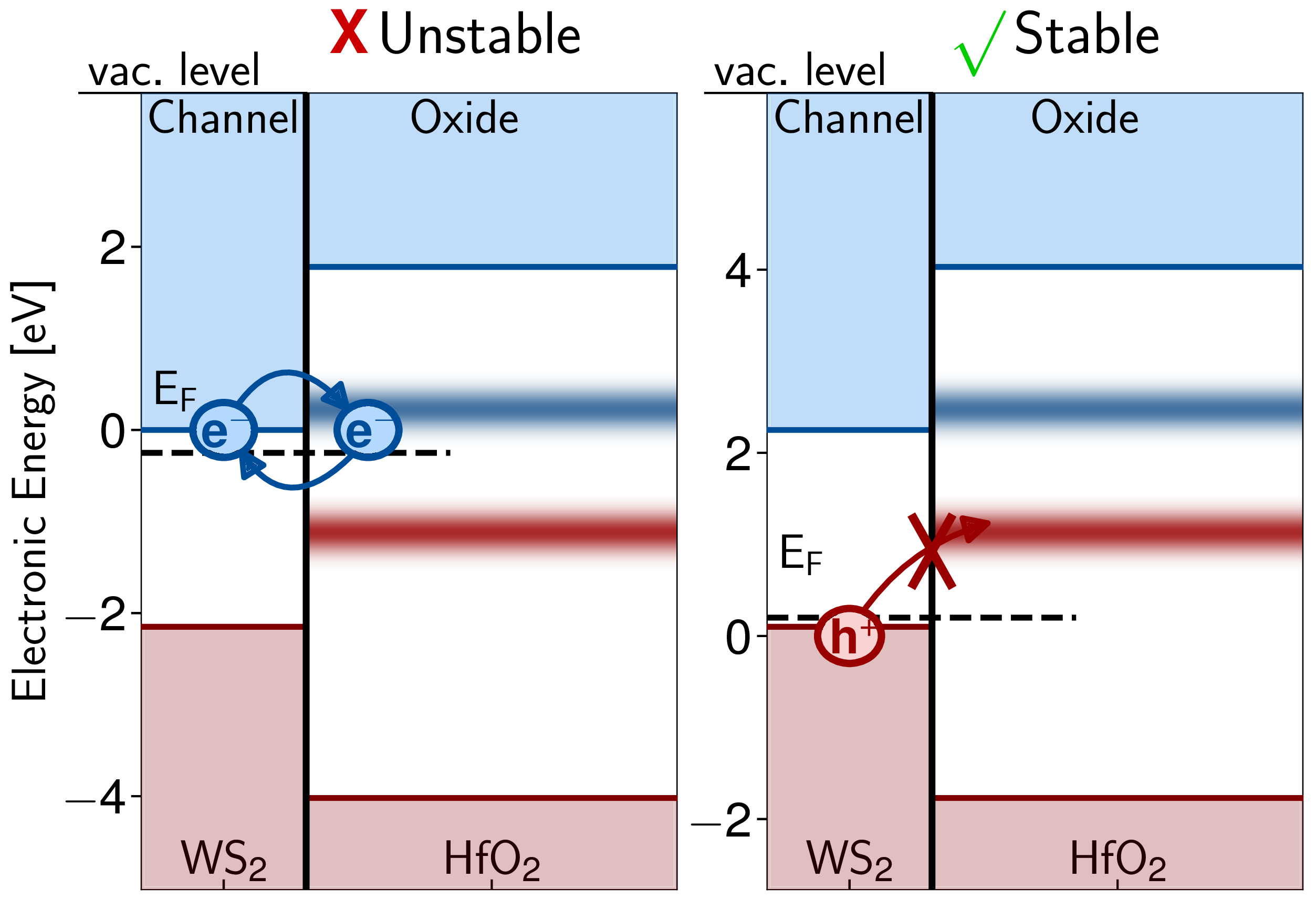
To improve device stability of 2D material-based field-effect transistors with amorphous gate oxides, the concept of Fermi-level tuning can be applied. By tuning the Fermi level in the channel, the energy distance between the charge carriers and the defect bands in the gate oxide can be increased. This way, the number of electrically active border traps is minimized without reducing the number of traps in the insulator. This approach is highly effective since charge trapping is strongly influenced by the energetic alignment of the Fermi level in the channel and the defect band in the insulator. In Fig. 1, the schematic of a WS2 FET with a HfO2 top-gate oxide is shown. If the Fermi level is aligned close to the conduction band, the majority of charge carriers are electrons in WS2, which dominate the current flow. However, as the conduction band edge of WS2 aligns with the electron-trapping defect band of HfO2, frequent charge transfer to oxide defects takes place. Alternatively, if WS2 was p-doped instead of n-doped (as shown in the right band diagram of Fig. 1), holes at the valence band edge would be the majority charge carriers. As the valence band edge of WS2 is located below the hole-trapping band in HfO2, the charging of oxide defects is highly unlikely. Therefore, p-doped WS2 in combination with a HfO2 gate oxide, has fewer electrically active oxide traps, leading to a stable threshold voltage during device operation. It is important to note that, for 2D semiconductors, charges are injected from the conduction or valence band edges. Hence, selecting a suitable combination of 2D semiconductor and insulator is critical, when designing a stable n-type or p-type FET.

Fig. 1: If the Fermi-level is aligned close to the conduction band edge, the device becomes electrically unstable due to frequent charge trapping events. However, when the Fermi-level is located close to the valence band edge (as depicted on the rightf) the FET shows stable operation.


