 |
|
||||
BiographyAleksandr Vasilev was born in Republic of Mordovia, Russia in 1990. In 2011 he obtained the Bachelor degree in Electronics and Nanoelectronics from Chuvash State University and the Master degree in Solar Heterostructure Photovoltaics at Saint Petersburg Electrotechnical University "LETI" in Russia in 2013. He joined the Institute for Microelectronics in October 2019, where he is working for the FWF project DEMOS and the CDL for SDS. His research focus will be on defect-centric modeling of reliability issues in SiC devices. |
|||||
Modeling the Hysteresis in the Current-Voltage Characteristics of Trench 4H-SiC MOSFETs
4H silicon carbide (4H-SiC) MOSFETs are increasingly replacing silicon (Si) in advanced power devices for several reasons. Among them are their capability to be operated at much higher temperatures, increased power density, higher maximum frequency, smaller size, and ability to be operated at voltages well above those applied for Si-based MOSFETs. Despite well-known fabrication processes of 4H-SiC, there is still a major issue regarding the reliability of the SiC/SiO2 interface due to the high defect density there, when compared to the Si/SiO2 interface. At the same time, the commonly used lateral MOSFETs are far away from state-of-the-art for commercially available 4H-SiC power MOSFETs. The new trend for the next generations of 4H-SiC power MOSFETs is in trench technologies due to their higher channel densities and, therefore, lower ON-resistances.
The main differences between planar and trench 4H-SiC MOSFETs are in the measured hysteresis behavior of Id-Vg curves. We assume that this is related to the density of trap states and their energy levels, which affect the kinetics of charge traps. To understand this behavior, a physical modeling approach, based on the Shockley-Read-Hall (SRH) theory for the interface defects, and the non-radiative multiphonon (NMP) theory for the defects in the oxide has been developed.
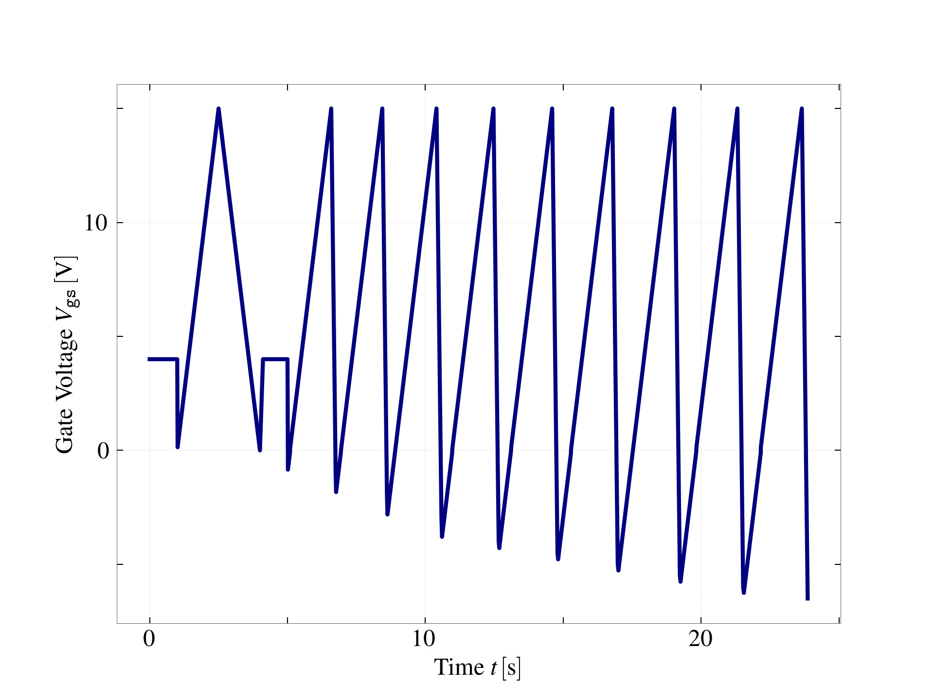
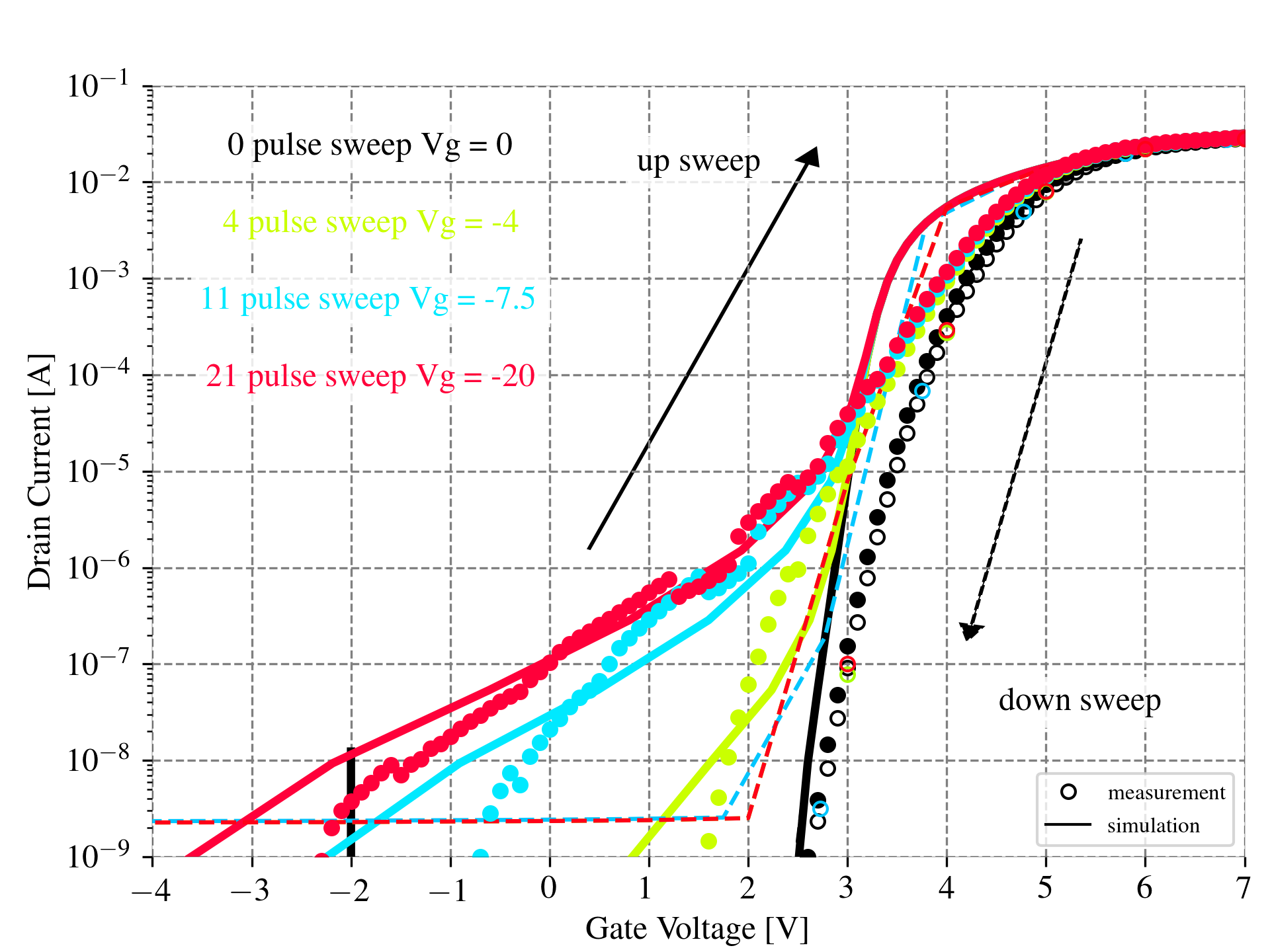
For measurements, we use a commercial discrete asymmetric trench 4H-SiC nMOSFET and assume an intended oxide thickness of 60 nm. The trench is fabricated by plasma etching. The n-channel a-face MOSFETs received a SiO2 layer, deposited via chemical vapor deposition with a subsequent post-oxidation anneal in a nitric oxide (NO) ambient. Fig. 1 shows the gate voltage (Vg) sweep scheme, starting at a positive gate bias stress of 4 V for 10 s. Subsequently, we apply zero pulse with a sweep rate of 1 V/s, sweeping up and down the gate bias within the range of 0 V to 15 V. After the second stress period, we apply the next 21 pulses with a sweep rate for the gate bias of 1 V/s for the up sweep and 10 V/s for the down sweep, and every period changes the starting negative gate voltage with the same final positive gate voltage. Fig. 2 shows a comparison between measured (symbols) and simulated (lines) Id-Vg curves at a temperature of 300 K and for different pulses. To obtain these results, we calculated the capture and emission times to investigate the effect of slow border traps on the charging dynamics. If the emission time at a higher gate bias is slower than the down sweep time and capture time, the charges are stored at the trap, which leads to the hysteresis effect. In addition, interface traps influence the sub-threshold slope, while positive bulk oxide defects compensate for the positive voltage shifts. The charge carrier mobility in the channel strongly depends on the selected plane of the crystal. In comparison with planar MOSFETs the fast donor-like interface defects are energetically located closer to the valence band and have an exponential distribution. The small trap concentrations, which are located close to the conduction band, lead to higher channel carrier mobilities in the trench due to the minor Coulomb scattering effect. In addition, the slow neutral acceptor-like border traps are energetically located in the mid-gap and demonstrate a Gaussian distribution. The carriers trapped at positive gate voltages are electrons, while the carriers trapped at negative gate voltages are holes. During sweeps at the high negative voltage, traps become positively charged and shift the threshold voltage towards negative gate voltages during each up sweep. The trapped electrons are unable to reduce the hysteresis width because of their low concentration.
Finally, our simulation results perfectly explain the hysteresis (see Fig. 2) indicating a high accuracy of our simulation models.

Fig. 1: Schematic view of the applied input gate voltage pulses.

Fig. 2: Measured (symbols) and simulated (lines) Id-Vg curves at a temperature of 300 K, while the low starting voltage level is varied and the high level remains constant.


