
 |
|
||||
BiographyMina Bahrami received her MSc. in condensed matter physics from the Amirkabir University of Technology of Tehran in 2021, where she studied a novel 2D material for the new generation of energy storage devices (i.e., lithium and sodium ion batteries). In June 2022 she joined the Institute for Microelectronics, focusing on ab-initio simulations of novel semiconductors and insulators in field-effect transistors. |
|||||
Defects in Strontium Titanate: A First-Principles Study
In recent years, high-k dielectrics have emerged as vital elements in the development of modern nanoelectronic devices. These materials play an important role in controlling the movement of charge carriers within the field-effect transistor's (FET) channel. In this context, SrTiO3 (STO) has been proposed as a potentially suitable gate dielectric for 2D material-based FETs. However, in order to ensure stable and reliable operation of, e.g., molybdenum disulfide (MoS2) FETs with STO as a gate insulator, it is crucial to understand the prevalent point defects in this material. The properties of these materials are primarily determined by the type and quantity of defects present in their lattices. Insulator defects are suspected to be responsible for hysteresis, bias temperature instabilities (BTI), and random telegraph noise (RTN) in metal-oxide-semiconductor field-effect transistor (MOSFET) devices because they can capture charges from the substrate during operation. These mechanisms involve charge transitions, which can be described as a non-radiative multiphonon (NMP) process.
In this work, we use density functional theory (DFT), employing a hybrid functional to determine crucial defect parameters such as the relaxation and formation energies and thermodynamic trap levels. These are the essential input parameters for physical charge trapping models based on NMP theory, enabling the prediction of degradation over the course of the device's lifespan. The four different defect candidates studied in this work are the oxygen vacancy VO, the strontium vacancy VSr, the titanium vacancy VTi, and the titanium antisite defect TiSr, as shown in Fig. 1. The defects were relaxed in all their possible charge states in order to confirm the existence of a specific state, where excess charge remains localized at the defect site.
These defects are expected to be relevant for the reliability of novel 2D devices. As illustrated in Fig. 2, depending on the 2D semiconductor used, the trap levels of these defects can be energetically close to either the valence or conduction band and thus act as electrically active charge trapping centers. For instance, depending on the defect's trap level, the titanium antisite defect can degrade the performance of MoS2 based devices.
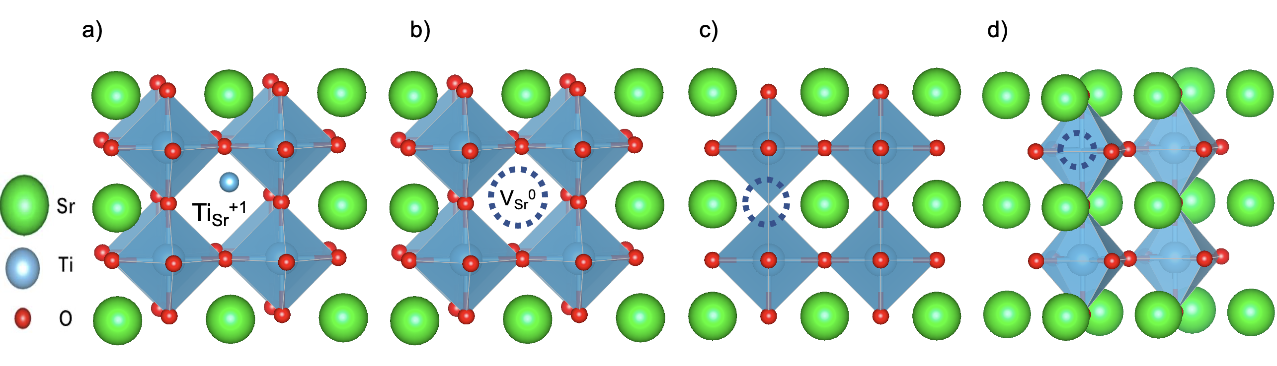
Fig. 1: The atomic structures of SrTiO3 with a) an antisite defect TiSr b) with a strontium vacancy VSr c) with an oxygen vacancy VO, d) with a titanium vacancy VTi.
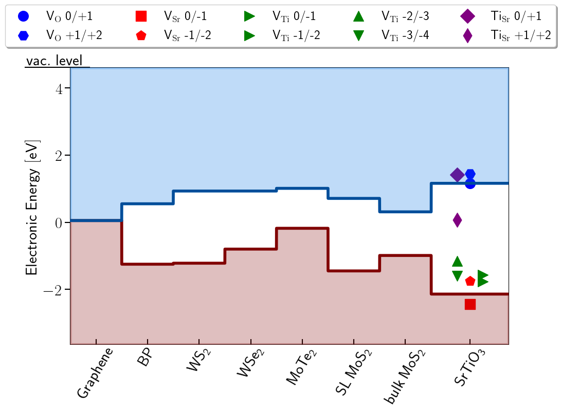
Fig. 2: Trap levels of the defects within the bandgap of SrTiO3 together with the band edges of commonly used 2D semiconductors in their bulk or single-layer (SL) form. VO trap levels are shown in blue, VSr in red, VTi in green, and TiSr in purple. The distance between the band edges and trap levels determines charge trapping and should be maximized for reliable devices.