
 |
|
||||
BiographyLukas Cvitkovich was born in 1992 in Eisenstadt, Austria. He received his Bachelor degree in Electrical Engineering and his Diplom-Ingenieur degree in Material Sciences from TU Wien, where he defended his Master Thesis in the Quantum Materials group of the Institute of Solid State Physics in 2019. During his studies, he also worked as a research assistant at the Institute of Sensor and Actuator Systems and at the Institute for Solid State Electronics at TU Wien. In May 2020 he joined the Institute for Microelectronics where he started his PhD studies, focusing on the ab initio simulation of oxide defects in semiconductor devices. |
|||||
Coherence Limit Due to Hyperfine Interaction with Nuclei in the Barrier Material of Si Spin Qubits
Semiconductor spin qubits are one of the most promising systems for implementing quantum computing on a large scale. In recent years, encouraging experimental demonstrations of one and two-qubit gates have been accomplished. Interactions with the environment impede coherent control of such a spin qubit. In this regard, hyperfine interactions between electron and nuclear spins impose a significant challenge. Silicon is a promising host material because it greatly enhances the spin coherence time by removing spinful 29 Si isotopes.
As more experiments rely on isotopic purification of Si, the role of other spinful atoms in the device should be clarified. As shown in the figure, interactions with atoms in the barrier layer of the gate-confined quantum dot are expected to contribute to the dephasing of the qubit state. Nevertheless, an accurate quantitative description of this phenomenon is still missing, as the hyperfine interactions with atoms in the barrier layers are poorly understood. We utilize density functional theory (DFT) to determine the hyperfine tensors between a conduction band electron in a Si quantum dot and a nuclear spin bath comprising atoms in the Si host lattice and the barrier layer. While previous ab initio studies focused on donor-bound or delocalized electrons in bulk systems, we consider realistic, disordered interfaces to which an external electric field confines an electron. Our models include the two most commonly used material systems, that is, 1) crystalline epitaxial Si/SiGe quantum wells and 2) amorphous Si/SiO2 (MOS) interface structures. This approach allows us not only to calculate the hyperfine interaction with 29Si, which is the dominant source of decoherence in natural Si, but also with 73Ge and 17O. The non-Si atoms show weaker interactions with the evanescent tail of the electron, which only becomes important for highly purified Si. Based on the DFT results, we estimate the dephasing time T2* due to magnetic noise from the spin bath and show that the coherence is limited by interactions with non-Si barrier atoms below a material dependent purification threshold.
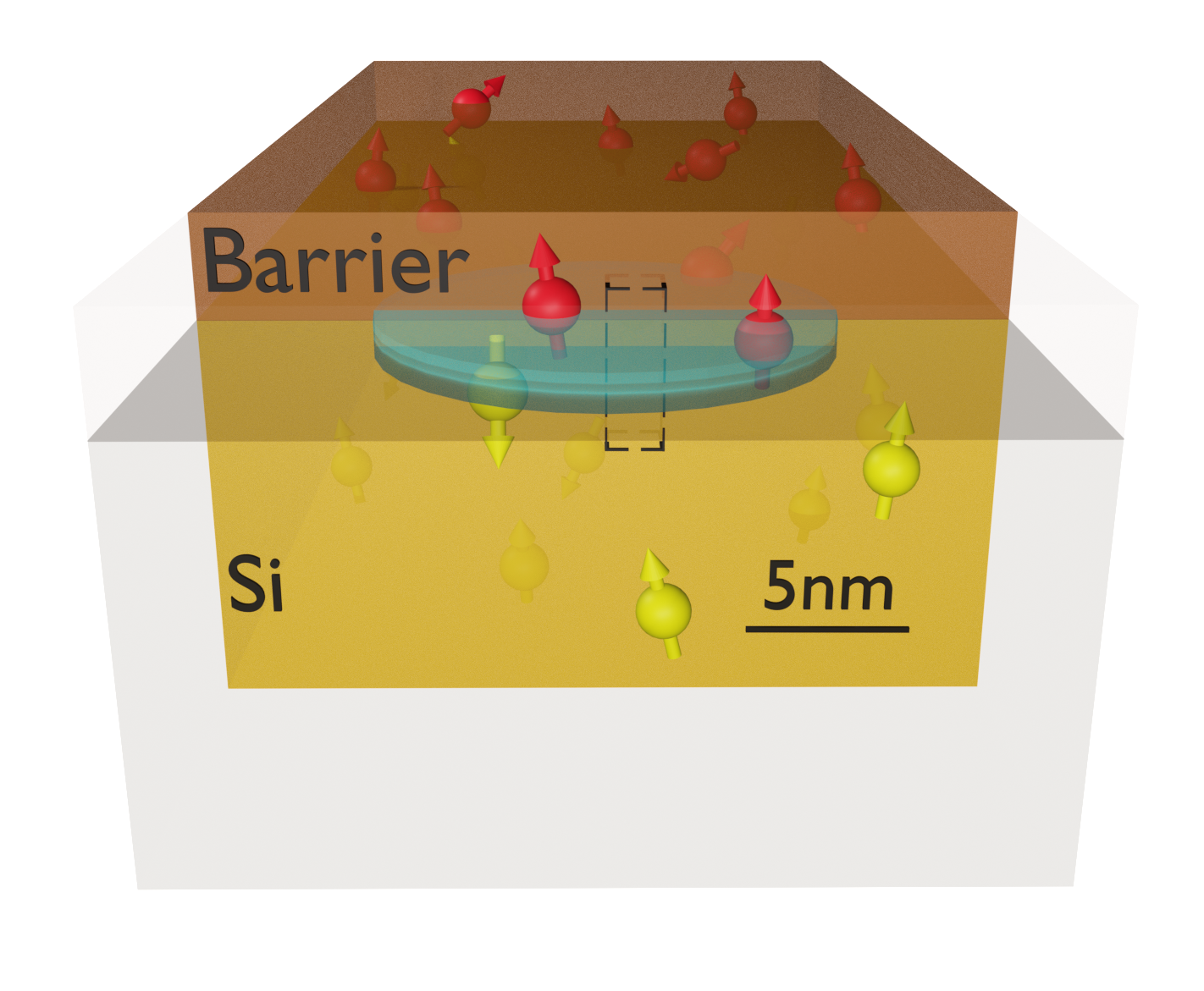
Fig. 1: Schematic device layout of a quantum dot (depicted as a blue ellipsoid) in a Si-based material stack. The dot is formed at the Si/barrier interface by top gates (not shown), which also confine the electron wavefunction in the lateral (xy) plane. Nuclear spins in both material layers (schematically represented as red and yellow arrows) act as a source of magnetic noise. The electron wavefunction amplitude at atomic nuclei mostly determines this interaction and the resulting decoherence.