
 |
|
||||
BiographyOliver Hartwig started to study Physics in 2011 at the Karlsruhe Institute of Technology where he obtained his BSc degree in 2015. In the same year he moved to Munich to continue his studies in Applied and Engineering Physics at the Technical University of Munich. In 2018 he graduated with an MSc degree, focusing on “On-Chip Photon Generation and Detection Using Two-Dimensional Materials Coupled to Plasmonic Waveguides”. During his PhD at the University of the Bundeswehr Munich (UBWM) in the Group of Prof. Georg S. Duesberg, Oliver worked on the synthesis and characterization of 2D materials. While being in the last stages of completing his dissertation at UBWM, Oliver joined the Institute for Microelectronics, TU Wien in May 2023. In collaboration with the UBMW, Oliver currently investigates the growth of fluorides and 2D materials by molecular beam epitaxy (MBE). |
|||||
Deposition of CaF2 Thin Films on TMDs and Metals
In semiconductor technology, improvements in integration density and performance of field-effect transistors (FETs) require downscaling of device size and especially the thinning of gate dielectrics. However, this imposes challenges such as control over material quality and layer thickness, especially for amorphous materials such as SiO2, Al2O3, and HfO2. Recent reports demonstrated epitaxial growth of ultra-thin (2.2 nm), crystalline CaF2 on Si(111), which promoted CaF2 as a promising candidate to overcome existing challenges in FET device fabrication. CaF2 is an ionic crystal with a lattice constant of 5.46 Å, matching that of silicon with 5.43 Å. It has a large band gap ( of SiO2 is 8.9 eV), a good permittivity of ε = 6.8 (ε of SiO2 is 3.9) and a high effective electron mass me = 1.0 m0 (vs. 0.42 m0 in SiO2). For device fabrication, achieving controlled crystalline growth of thin CaF2 layers on metals or graphitic materials is highly desirable, as these substrates can serve as contact electrodes. Additionally, the direct growth of CaF2 on various semiconductors holds significant promise for advancing FETs based on materials beyond silicon. The growth of a crystalline CaF2 layer depends on the meticulous and gradual evaporation of CaF2 films in an ultrahigh vacuum environment (UHV). Molecular Beam Epitaxy (MBE) systems are typically the most effective in meeting the technical requirements for this process. Our research aims to establish controlled growth procedures, resulting in ultra-thin (< 3 nm), closed, and pinhole-free CaF2 films on metallic substrates. The morphology of the CaF2 films is studied by AFM scans, as shown in Fig. 1. A relatively thick (18 nm) CaF2 layer was deposited on a gold surface by evaporation. A low RMS roughness of 0.7 nm could be determined for the CaF2 film, which is only marginally larger than the underlying gold film's low RMS roughness of 0.35 nm. Conductive AFM scans confirmed that the film fully covers the gold surface. Deposition of gold electrodes on top of the CaF2 is then carried out to enable capacitance measurements. We are currently investigating the deposition of much thinner (< 3 nm) CaF2 films while maintaining full surface coverage.
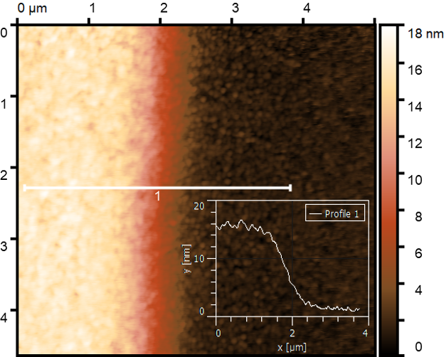
Fig. 1: AFM scan of a CaF2 film deposited on a gold substrate.