
 |
|
||||
BiographyPedram Khakbaz was born in Arak, Iran. He received his Ph.D. degree in electronics engineering from the University of Udine, Italy, in 2022 where he studied the electronic transport in devices based on two-dimensional semiconductors. From Sep. 2016 to Sep. 2018, he was with the computational nano-electronics lab and finished his M.Sc. degree in nano and micro-electronics engineering at the University of Tehran, Iran. In June 2022, Pedram joined the Institute for Microelectronics as a postdoctoral researcher and his current research interests include ab initio modeling and quantum transport for the modelling of devices based on 2D semiconductor materials. |
|||||
2D Bi2O2Se and Its Native Oxides: First-Principles Study
Semiconductor and dielectric research has witnessed significant advancements, introducing significant prospects for the electronics industry. A notable breakthrough revolves around the systematic layer-by-layer oxidation of Bi2O2Se, a layered semiconductor, leading to the formation of an atomically thin gate dielectric, bismuth selenite (Bi2SeO5). This controlled oxidation leads to the creation of the native oxide dielectric, paving the way for making high-quality planar and FinFET Bi2O2Se devices. Leveraging this innovation, the produced dielectric retains its single-crystalline nature, forming an atomically flat, nearly lattice-matched interface with Bi2O2Se. A remarkably low interfacial trap density characterizes this smooth interface. By harnessing advanced UV photolithography, selective oxidation becomes attainable, enhancing the versatility of this material combination. The single-crystalline β-Bi2SeO5 is distinguished by a large out-of-plane dielectric constant of around 35, coupled with superior insulative attributes. Consequently, this has facilitated the realization of top-gated two-dimensional field-effect transistors (2D FETs) with sub-0.5 nm equivalent oxide thickness (EOT) dielectrics, showcasing leakage currents below 0.015 A cm-2 at 1 V, in alignment with the rigorous 2021 IRDS standards. While these achievements are commendable, there is an obvious void in our comprehensive understanding. Although myriad experimental analyses have been undertaken, fundamental details like precise crystal structures and intrinsic material properties are still missing. To bridge this gap, we have utilized Density Functional Theory and Density Functional Perturbation Theory to study the structural, electronic, and dielectric properties of Bi2O2Se and its native insulators. Our intent is clear: to deliver well-articulated foundational knowledge and establish a robust platform for future research, catering to experimentalists and theoreticians.
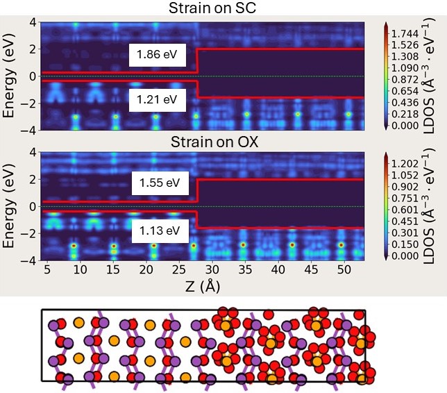
Fig. 1: Band alignment between the semiconductor and oxide (β-Bi2SeO5). Due to their non-lattice-matched nature, a decision must be made about applying strain to either the semiconductor or the oxide. Straining the oxide is a preferred approach.
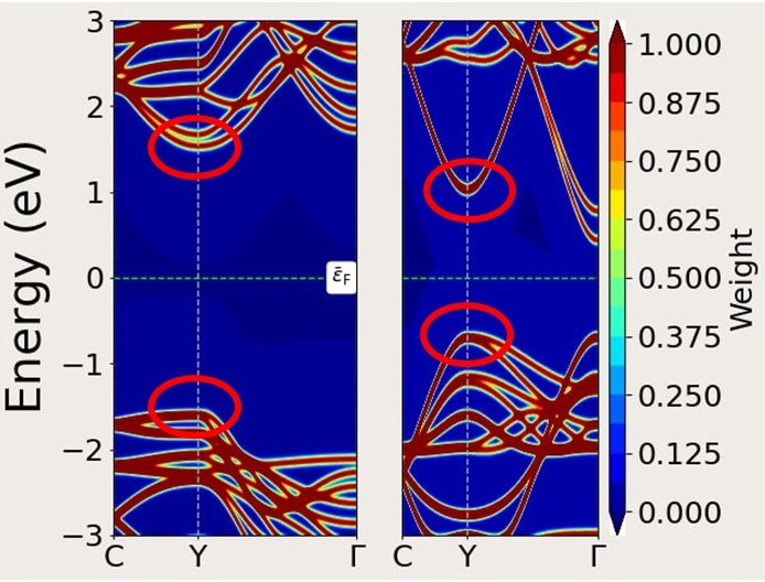
Fig. 2: Equivalent energy states at different valleys in the band structure of materials. The left figure depicts the oxide, while the right figure shows the semiconductor valley degeneracy.