
 |
|
||||
BiographySabine Leroch obtained her M.Sc. and doctoral degrees at TU Wien at the Institute of Theoretical Physics, after which she took a post-doctoral position at the Universidad Compludense de Madrid. She has many years of experience in classical molecular dynamic simulations in different fields and for a broad set of applications. She was previously employed as a post-doctoral researcher at the University of Natural Resources and Applied Life Sciences (BOKU) Vienna, in the field of bio-chemical engineering and as senior scientist at the Austrian Competence Center of Tribology. At the Institute for Microelectronics, Sabine is working in the Christian Doppler Laboratory for Multi-Scale Process Modeling of Semiconductor Devices and Sensors, where she is in charge of the atomistic description of physical processes taking place during the fabrication of semiconductor devices. In particular, she is investigating the implantation and activation of dopants in silicon carbide (SiC). |
|||||
The Impact of Implantation Conditions on the Dopant Activation and Annealing of Defects
Silicon carbide (SiC) is an important material for future green technologies. Compared to silicon, it exhibits higher energy efficiency, lower power losses, and compact design when applied in high-power devices and sensors. 4H-SiC is a widely used semiconductor because of its high crystalline quality, wide bandgap of 3.2 eV, large breakdown field, and exceptional thermal and mechanical stability. SiC is conventionally doped with electron donor or acceptor atoms such as N or Al to improve its conductivity. For them to be electrically active, these dopants should occupy perfect lattice sites in crystalline SiC and provide states in the bandgap close to the valence band in the case of Al and close to the conduction band in the case of N, adding holes or electrons there, respectively.
Traditionally, dopants are introduced using ion implantation, i.e., the ions are accelerated towards the SiC wafer with a predefined energy and incident angle, as shown in Fig. 1. This physical and random implantation process damages the SiC crystal. It ensures that the ions are not immediately localized on SiC lattice sites; rather, they are typically found in arbitrary positions in the crystal. Moreover, the interaction with the high-energy ions causes silicon and carbon atoms to be displaced from their original positions. These displaced atoms represent defects that severely degrade the conductivity of the semiconductor. Therefore, process engineers try to minimize defect creation during implantation by low-dose implantation or by implanting at elevated temperatures. High-temperature annealing is a necessary step after implantation to further reduce the number of defects and achieve a high number of activated dopants.
To shed more light on the generated defect structures and their impact on the Al activation, we perform molecular dynamic (MD) simulations for the implantation and subsequent annealing. We achieved a good qualitative agreement with experiments concerning the dose and temperature-dependent defect fractions, the re-crystallization energy, the fraction of activated Al ions, and the annealing temperature. In Fig. 2 and Fig. 3, the SiC structures are visualized for dopant doses of 1x10¹⁴/cm² and 7.5x10¹⁴/cm², respectively. The top images show the SiC structure immediately after implantation. In contrast, the bottom images depict the final material after annealing at 2300 K. Implantation at room temperature and at 800 K are studied, as shown on the left and right of the same figures, respectively. Large defect areas in the crystal are shown in gray, which shrink to small defect clusters after annealing. Although there are fewer defects in SiC immediately after implantation at higher temperatures, more Al atoms are located at lattice sites (activated) after implanting at 300 K than at 800 K at the end of annealing.
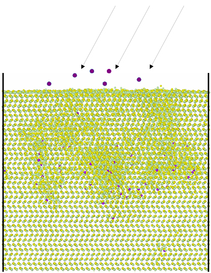
Fig. 1: 4H-SiC directly after implantation, with Al shown in purple, Si in green, and C in yellow.
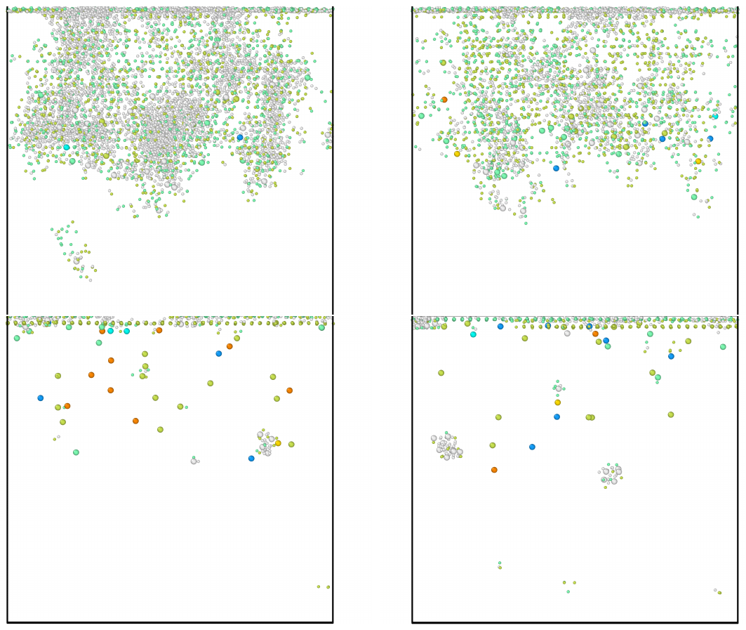
Fig. 2: Top: Defect structure directly after Al implantation with a dose of 1x10¹⁴/cm² at 300 K (left) and 800 K (right).
Down: Defect structure directly after annealing at 2300 K with a dose of 1x10¹⁴/cm² at 300 K (left) and 800 K (right).
The grey region depicts the atoms displaced from their lattice sites; the large spheres are Al, while the small ones are Si- and C-related defects.
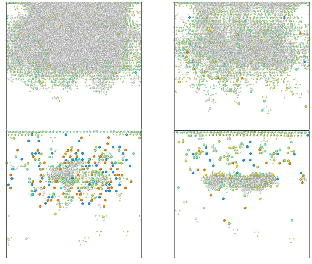
Fig. 3: Top: Defect structure directly after Al implantation with a dose of 7.5x10¹⁴/cm² at 300 K (left) and 800 K (right).
Down: Defect structure directly after annealing at 2300 K with a dose of 7.5x10¹⁴/cm² at 300 K (left) and 800 K (right).
The grey region depicts the atoms displaced from their lattices sites, the large spheres are Al, while the small ones are Si- and C-related defects.