
 |
|
||||
BiographyMohammad R.A. Monazam received his PhD. from Johannes Kepler University in Linz where he studied optical properties of semiconductors. He then continued to work at the Zentrum für Oberflächen- und Nanoanalytik (ZONA) as a theoretical physicist. As a post doctoral researcher he joined the Physics of Nanostructured Materials group of Jani Kotakoski located at Vienna university. There he studied two dimensional materials with the main focus on defect creation mechanisms, doping and atom manipulations. In June 2023 he joined the research group of Prof. Grasser studying defects in 2D materials and their impact on potential device applications using ab-initio electronic structure methods. |
|||||
Native Defects in β-Bi2O5Se: Ab initio Study
While silicon has been dominant in microelectronics, it faces limitations at sub-10 nm nodes. To address these scaling challenges, two-dimensional (2D) semiconductors, with their intrinsic atomic thickness, flexibility, and dangling-bond-free surfaces, are emerging as competitive candidates for next-generation electronics. A two-dimensional semiconductor such as Bi2O5Se offers promising alternatives due to their high carrier mobility, moderate band gap, stability, and positive mechanical properties. However, most 2D semiconductors lack the insulating quality required for sub-1-nm equivalent oxide thickness (EOT) gate dielectrics in 2D transistors.
Integrating high-mobility 2D semiconductor channels with ultrathin high-κ dielectrics can counteract short-channel effects in field-effect transistors (FETs), offering higher speed, lower power consumption, and increased integration density. However, it is very challenging to integrate 2D semiconductors with dielectric layers that have very small EOTs and low leakage current requirements. The recent direct synthesis of native oxide dielectrics on semiconductors shows promise for advanced device fabrication. The β-Bi2O5Se phase made by the UV-assisted intercalative oxidation method leads to a single-crystalline device with an atomically flat lattice-matched interface with low trap density at the Bi2O2Se interface. It has been shown that β-Bi2O5Se with a mere thickness of 0.41 nm has a leakage current less than 0.015 A at 1 V bias.
Despite undergoing a meticulous and intricate synthesis process, materials are still afflicted by inherent native defects. Native defects within semiconductors and insulators wield significant influence over the functionality of electronic devices, their impacts varying depending on the defect's nature. These defects can introduce supplementary energy levels within the band gap, thereby limiting the material's electrical conductivity. Acting as traps for charge carriers, they instigate heightened carrier scattering and consequent reductions in mobility, thereby impeding device performance.
In our investigation, we embark on a comprehensive exploration of the native defects that are anticipated to populate the β-Bi2O5Se material. Central to our inquiry are oxygen vacancies, a class of defects ubiquitous in oxide materials known for their profound influence on material properties. While oxygen vacancies have long been recognized as pivotal players in semiconductor technology, notably implicated in Bias Temperature Instability (BTI), their significance transcends conventional silicon-based systems, extending to a diverse array of materials.
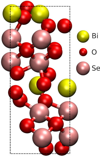
Fig. 1: Unit cell of β-Bi2O5Se .