
 |
|
||||
BiographyRoberto Lacerda de Orio studied electrical engineering at the University of Campinas (UNICAMP), Brazil, where he received his Bachelor degree in 2005 and his Master degree with emphasis on Microelectronics in 2006. He joined the Institute for Microelectronics in October 2006, where he received his doctoral degree in 2010 and worked as a post-doctoral researcher until 2013, with a focus on reliability issues in interconnects of integrated circuits. From 2014 to 2018 he was a tenured Assistant Professor at the Faculty of Electrical and Computer Engineering (FEEC) of UNICAMP, where he carried out research, teaching, and supervision activities of students at all academic levels in the area of micro- and nanoelectronics, mainly on topics related to the reliability of integrated circuits as well as the modeling, simulation, and fabrication of semiconductor devices. He was a Principal Investigator in research funded projects and also acted as Deputy Head of the Department of Semiconductors, Instruments and Photonics at FEEC/UNICAMP. In October 2018 he rejoined the Institute for Microelectronics as a research scientist (Postdoc) working on non-volatile magnetoresistive memory devices and supporting teaching activities. He has many years of experience in developing numerical simulation tools for micro- and nanoelectronic devices with programming skills in Python, C, and C++. Roberto is currently a Senior Scientist and is supporting the research related to robustness of electronic circuits, with a focus on the analysis of semiconductor physical phenomena and their reliability. He is also involved in lecturing for the Bachelor and Master programs at the Institute for Microelectronics, which includes programming in C, microelectronic devices simulation, modeling of electronic devices, and simulation of semiconductor devices fabrication. |
|||||
Switching Efficiency of a Spin-Orbit Torque MRAM Assisted by Voltage-Controlled Magnetic Anisotropy
The switching of a three-terminal magnetoresistive random access memory (MRAM) cell based on spin-orbit torque (SOT) with the support of voltage control of magnetic anisotropy (VCMA) and spin-transfer torque (STT) has considerable potential for ultrafast, low-power operation, making it particularly promising for cache memories, in replacement of conventional CMOS-based SRAM.
The impact of the combination of these mechanisms on the critical current for magnetization switching as a function of the applied voltage across the magnetic tunnel junction (MTJ) composing the cell is shown in Fig. 1. In this case, a positive bias reduces the magnetic anisotropy, which leads to a reduction of the energy barrier for switching and, as a result, a lower critical current is required for switching.
The reduction of the critical current implies a reduction of the energy required for the SOT bias. This can be verified in Fig. 2, which shows the energy associated with the SOT current pulse, the energy dissipated by the MTJ, and the total energy required for switching as a function of the voltage applied across the MTJ. As for positive voltages, the critical current is reduced, and the energy required for SOT is also reduced. However, the applied voltage results in a current flow through the MTJ, leading to power consumption. Thus, on the one hand, the applied bias helps to reduce the energy for SOT due to the VCMA effect; on the other hand, it leads to additional energy dissipation through the MTJ. The black curve in Fig. 2 shows the total switching energy, which indicates that a compromise between both contributions has to be considered in selecting the applied voltage so that a minimum energy for switching can be achieved.
However, to evaluate the efficiency of the switching scheme as a whole, the switching speed has to be taken into account, in addition to the required energy. For that purpose, we apply the switching energy-time product (ETP) as a figure of merit. The resulting ETP as a function of the applied voltage is shown in Fig. 3. From this figure, an optimal bias can be determined, for which the SOT-MRAM operation is most efficient, meaning that fast switching with reduced energy consumption can be achieved simultaneously.
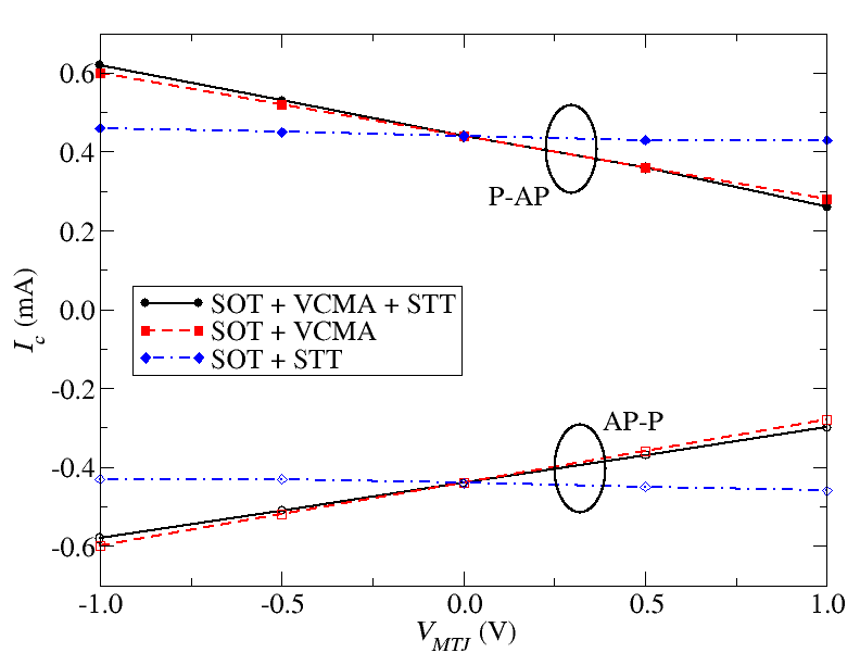
Fig. 1: Critical current as a function of the voltage across the MTJ considering different mechanisms acting on the SOT-MRAM cell.
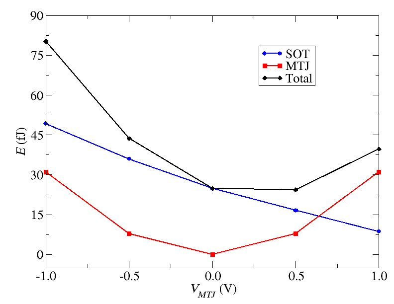
Fig. 2: Energy consumed due to the applied current for SOT, energy dissipated by the MTJ, and the total energy required for the magnetization switching as a function of the voltage applied across the MTJ.
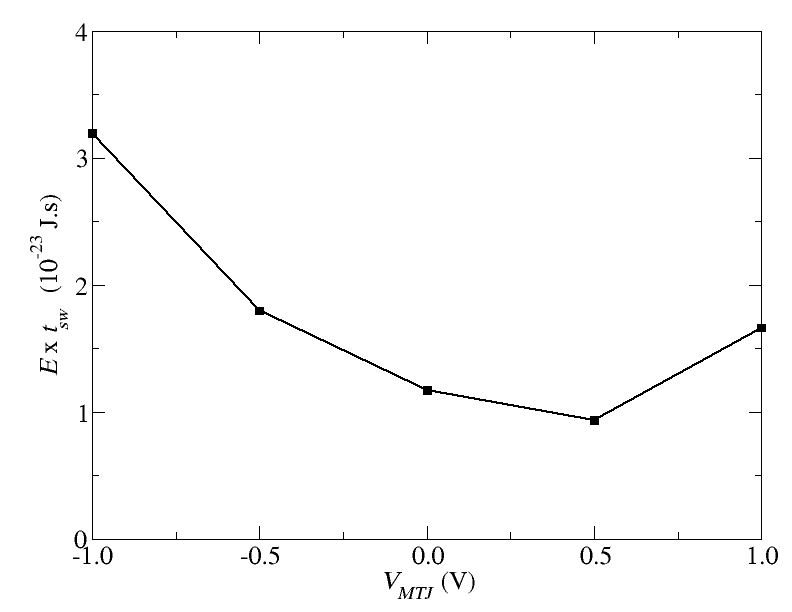
Fig. 3: Switching energy-time product as a function of the applied bias across the MTJ.