
 |
|
||||
BiographyTobias Reiter obtained his Master's degree (Dipl.-Ing.) in Technical Physics in 2022 and is currently completing the inter-faculty Master Program (MSc.) Computational Science and Engineering, both at TU Wien. He joined the IµE as a doctoral candidate in 2022, where he is working on semiconductor process simulation. His current research focuses on the development of the process simulation library ViennaPS, where he is developing models for novel etching and deposition processes for semiconductor fabrication. He is also part of the Christian Doppler Laboratory for Multi-Scale Process Modeling of Semiconductors Devices and Sensors. |
|||||
Modeling Oxide Regrowth During Etching of Vertical 3D NAND Structures
Vertical three-dimensional (3D) NAND flash memory has emerged as a leading technology in non-volatile storage devices, offering high-density data storage in a compact form factor. Its architecture involves stacking memory cells vertically, enabling increased storage capacity with a small footprint. However, the fabrication of such structures is challenged by the intricacies of the manufacturing processes, necessitating a profound understanding of the underlying physical phenomena.
One of many crucial processing steps during the fabrication of 3D NAND flash memory structures is the selective etching of Si3N4 in the presence of SiO2. This process has been shown to cause the redeposition of byproducts on the SiO2 layers in wet etching solutions, as shown in Fig. 1. This redeposition can significantly hinder further processing steps and ultimately impact performance. To address this, we devised a physical model capable of clarifying the byproduct generation and mass transfer dynamics, mirroring experimental observations of the oxide regrowth behavior.
Our model employs a hybrid approach, integrating the Level-Set method to accurately track surface evolution and a Cell-Set framework to monitor volumetric changes around the surface. Specifically, it simulates the transient convection-diffusion of etching byproducts in the wet etching solution, considering convection induced by stirring and incorporating a sink term to mimic byproduct removal. The accumulated concentration of resulting byproducts is tracked over each time step, and the distribution of this byproduct around every surface point informs the amount of redeposition, ultimately dictating the growth rate of the oxide.
The model, parameterized by five key variables calibrated against experimental data, was applied to a 128-layer stack, as illustrated in Fig. 2. Notably, it revealed differential byproduct distribution within the stack, with increased accumulation observed at lower layers due to slower escape to the bulk etching solution. Consequently, enhanced oxide regrowth rates were observed at the bottom. Understanding these nuances helps to fine-tune the manufacturing process, ensuring that each layer of the 3D NAND memory performs optimally.
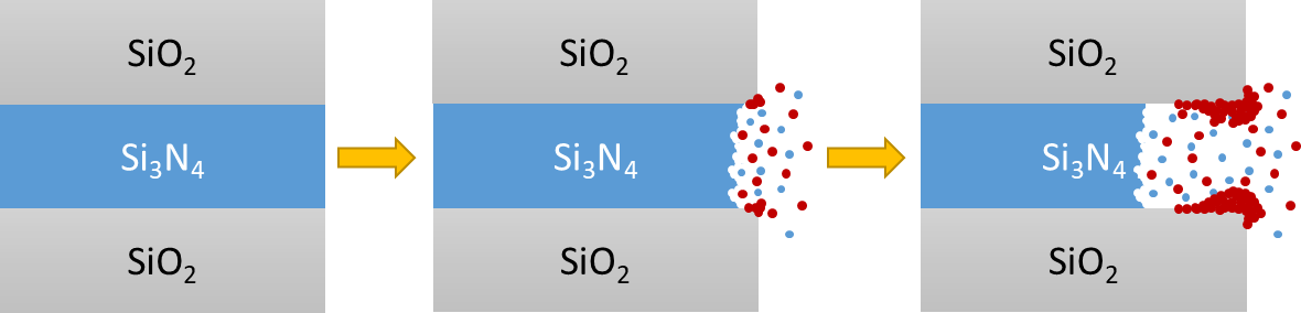
Fig. 1: Schematic depiction of oxide regrowth from generated byproducts (red circles) during Si3N4 (blue film and circles) etching.
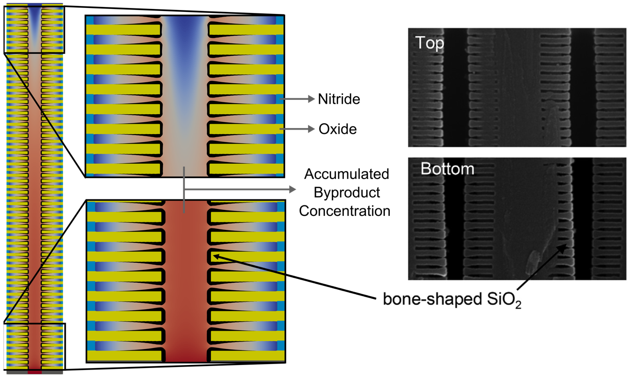
Fig. 2: Results of the selective etching and redeposition simulation in a 3D NAND stack with 64 Si2O (yellow)/Si3N4 (blue) pair-layers. The redeposited oxide (black) is shown on the Si2O layers, while in between the materials, the final byproduct concentration is shown. The results are compared to experimental studies (T. Kim et al., Microelectronic Engineering, vol. 221, 2020).