
 |
|
||||
BiographyMauro Borghi was born in 1995 in Reggio Emilia, Italy. He completed his Bachelor's Degree in Mechanical Engineering and Master's Degree in Materials Engineering from the University of Modena and Reggio Emilia. He performed his thesis work at Helmut Schmidt University, Hamburg. He joined the Institute for Microelectronics in 2022, where he is working on the growth and characterization of fluorides for 2D nanoelectronics in collaboration with the University of Modena and Reggio Emilia. |
|||||
Molecular Beam Epitaxy of Fluorides on Conductive Materials
Innovation in insulating materials for field-effect transistors (FETs) is essential to overcome the physical limitations imposed by the traditional silicon/silicon dioxide (Si/SiO2) combination. Fluorides, such as strontium fluoride (SrF2) and calcium fluoride (CaF2), have been identified as the most promising materials for this purpose. These ionic crystals allow the creation of FET devices with superior performance, as they have a high dielectric constant and a wide bandgap, and their surfaces are inert because they are terminated with fluorine atoms. These peculiarities increase the performance and reliability of the transistor. To completely break away from silicon and make the continued miniaturization of devices feasible, gaining experience in growing fluorides on conductive materials, such as metals, or two-dimensional conductors, such as graphene, is essential. Experimentally, graphene is replaced by a substrate called highly oriented pyrolytic graphite (HOPG), formed by many layers of graphene stacked on top of each other. HOPG is used because it is straightforward to clean and can be exfoliated using adhesive tape. Furthermore, it is easier to handle than a single layer of graphene.
The growth of these insulators must take place in ultra-high vacuum (UHV – base pressure 2.0×10⁻¹⁰ mbar) chambers to avoid any contamination, which could degrade the material's properties. These chambers are also necessary to increase the mean free path of the molecules during the deposition process through molecular beam epitaxy (MBE). This controlled environment is crucial for obtaining high-quality thin films and ensuring a clean and well-defined interface between the insulator and the conductive substrate.
To characterize and evaluate the quality of these thin films and their interfaces, advanced surface characterization methods are employed, such as X-ray photoelectron spectroscopy (XPS), ultraviolet photoelectron spectroscopy (UPS), high-energy electron diffraction (RHEED), and atomic force microscopy (AFM). These techniques allow for the analysis of the films' chemical composition, crystal structure, and surface morphology, providing valuable information on the electronic properties and interface quality, which are crucial for the performance of FET devices.
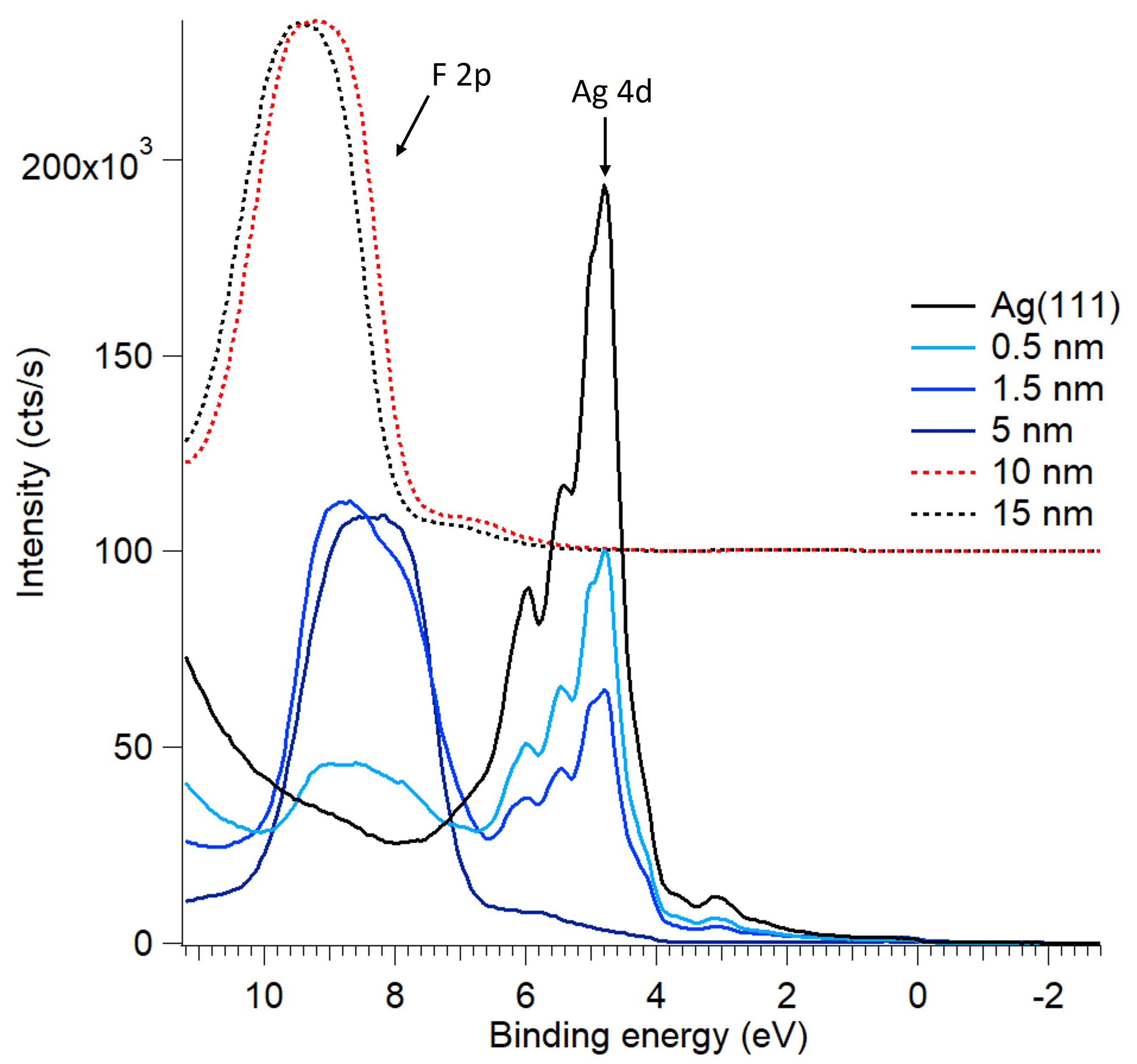
Fig. 1: UPS spectra recorded as a function of SrF2 thickness, deposited at RT. The spectra acquired at 10 nm and 15 nm of nominal thickness are shifted vertically by 100 kCounts/s for clarity. The spectrum of the clean surface is dominated by the emission from the 4d band of Ag(111). As soon as SrF2 is deposited on the surface, the broad emission from the fluoride F 2p valence band gradually increases. [M. Borghi et al., Applied Surface Science 656 (2024)]
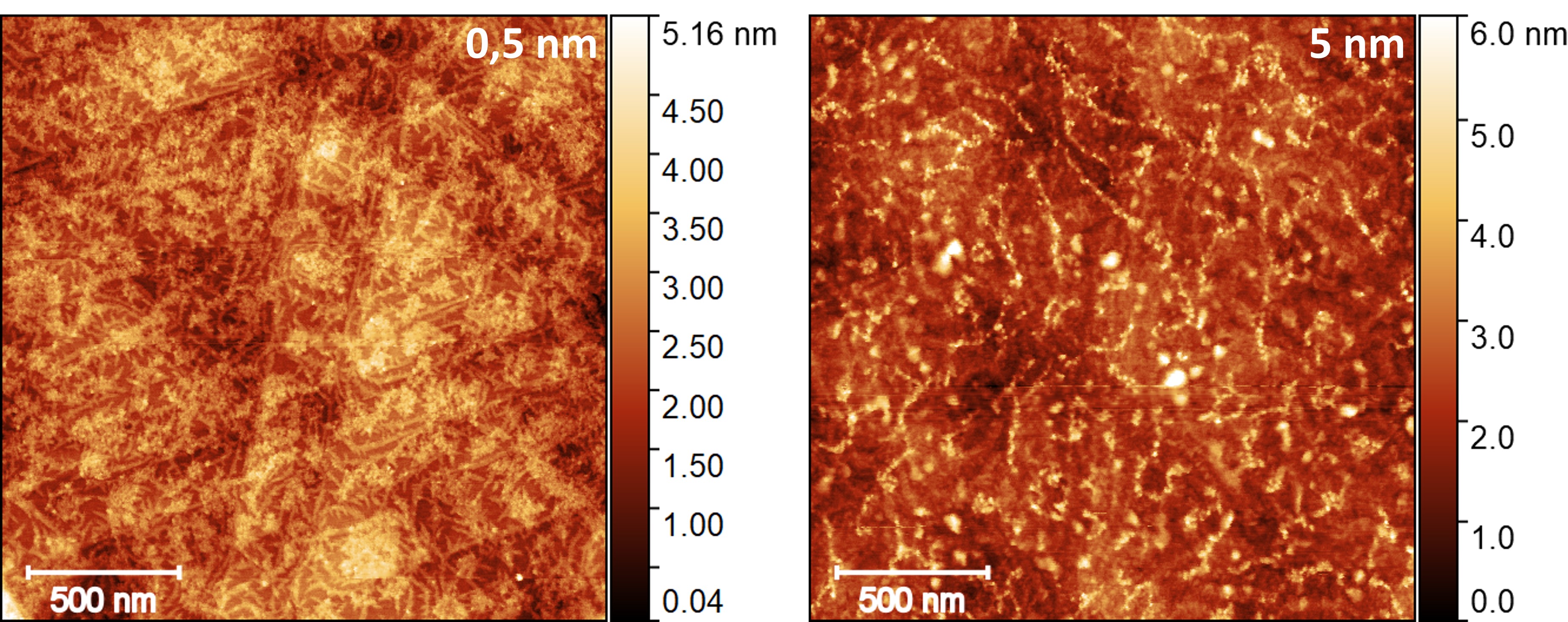
Fig. 2: AFM image (2 × 2 μm) after the deposition of 0.5 nm (left image) and 5 nm (right image) of SrF2 at RT in morphology contrast. The 0.5 nm thickness shows the typical dendritic growth of fluorides deposited on metals. After depositing 5 nm of fluoride, the substrate appears completely covered. [M. Borghi et al., Applied Surface Science 656 (2024)]