
 |
|
||||
BiographyHajdin Ceric was born in Sarajevo, Bosnia and Herzegovina, in 1970. He studied electrical engineering at the Electrotechnical Faculty of the University of Sarajevo and the Technische Universität Wien, where he received the degree of Diplomingenieur in 2000. In 2005 he received his PhD in technical sciences and in 2015 his venia docendi (habilitation) in microelectronics from the Technische Universität Wien. He is currently an Associate Professor at the Institute for Microelectronics. His research interests include finite element method modeling and simulation in microelectronics, application of machine learning in computer numerics, atomistic modeling in material science, electromigration in metals, and mechanical reliability of metals and semiconductors. In 2010 he was appointed the head of the Christian Doppler Laboratory for Reliability Issues in Microelectronics with two participating industrial partners: ams AG and Infineon Technologies Austria AG. Dr. Ceric participated in several European Community and FFG projects. In his research, Dr. Ceric has been closely cooperating with a company SOITEC, France, and research center imec, Belgium. He is a reviewer for several American Institute of Physics, Elsevier, and IEEE journals. Research Topics:Interconnect Reliability |
|||||
Enhancing Interconnect Reliability by Nano-Twinned Grains
Twin boundaries are not uncommon in nature and can be formed by different physical or chemical processes in various metals and alloys. Understanding and uncovering mechanisms of twin boundary formation remains an intense area of research. They are formed as a single plane of atoms between two non-mixing phases due to the need for minimum interfacial energy. Such a single plane demands a small amount of additional energy. Understanding the association between defects in a material and the resulting material properties is a current research challenge in materials science. In this respect, exploring materials containing nanotwins can open new avenues for research and applications. The presence of twin boundaries has a significant impact on electromigration reliability. The triple points where twin boundaries meet a grain boundary slow down the electromigration-induced atomic migration by an order of magnitude. Also, the electromigration-induced void growth rate for the copper grain containing nanotwins is calculated to be approximately one order of magnitude lower than that for the twin-free copper grain.
The first objective of our study is to investigate polycrystalline copper interconnect structures that contain nanotwins utilizing physical modeling and simulation. The study comprises the effect of geometry, scale, annealing temperature, annealing time, and mechanical stress on the transformation of the copper microstructure, i.e., grain growth and the emergence of nanotwins. The interconnect layouts and geometries in focus are redistribution layers of nano interconnects. The presence of specific polycrystalline structures containing nanotwins will change the mechanical properties of interconnect components and, consequently, their response to different temperatures and mechanical loads. The phenomenon in focus impedes void growth and migration by the presence of nano twins.
The Monte Carlo Potts algorithm is the natural choice for modeling grain growth. This project uses the Monte Carlo Potts (MC-P) simulation to obtain the grain boundary structure for a given interconnect geometry after annealing at the prescribed temperature and for the prescribed duration. In the subsequent step, a twin boundary seed is set into some chosen grain, and the growth and expansion of nanotwins are simulated on the atomic scale by the Monte Carlo – Gilmer Bennema (MC-GB) algorithm (see Fig. 1).
These results obtained by simulation of grain boundary and nanotwins development are used as an input for electromigration reliability simulations. In the scope of our work, the reliability issue in focus is the phenomenon of electromigration-induced voiding. The effect of nanotwins on nucleation, growth, and migration of voids is investigated (see Fig. 2).
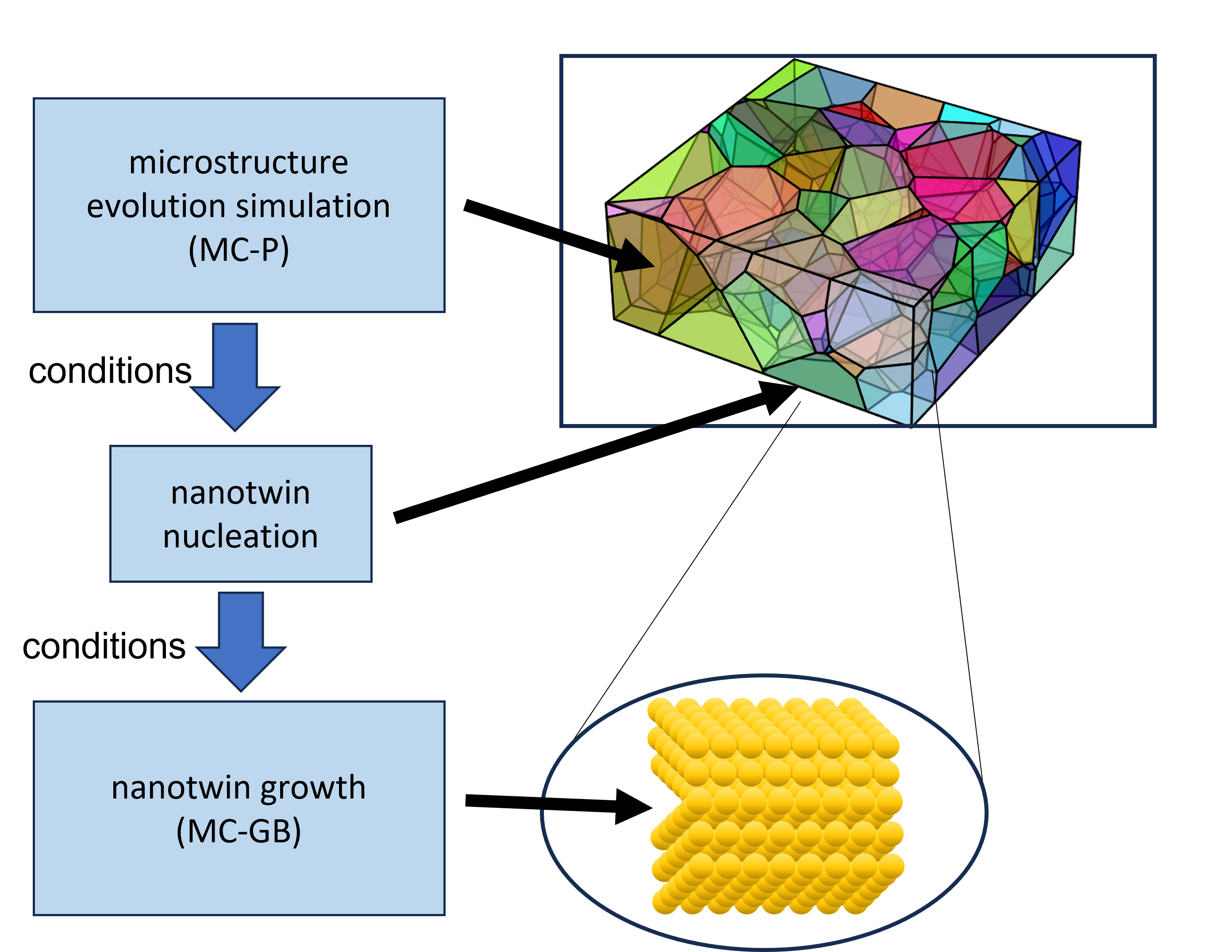
Fig. 1: Overall simulation scheme for microstructure and nanotwin growth: After the microstructure simulation, the conditions for the nucleation of a nanotwin are set. Depending on the nucleation position and under the influence of temperature, the nanotwin growth is initiated.
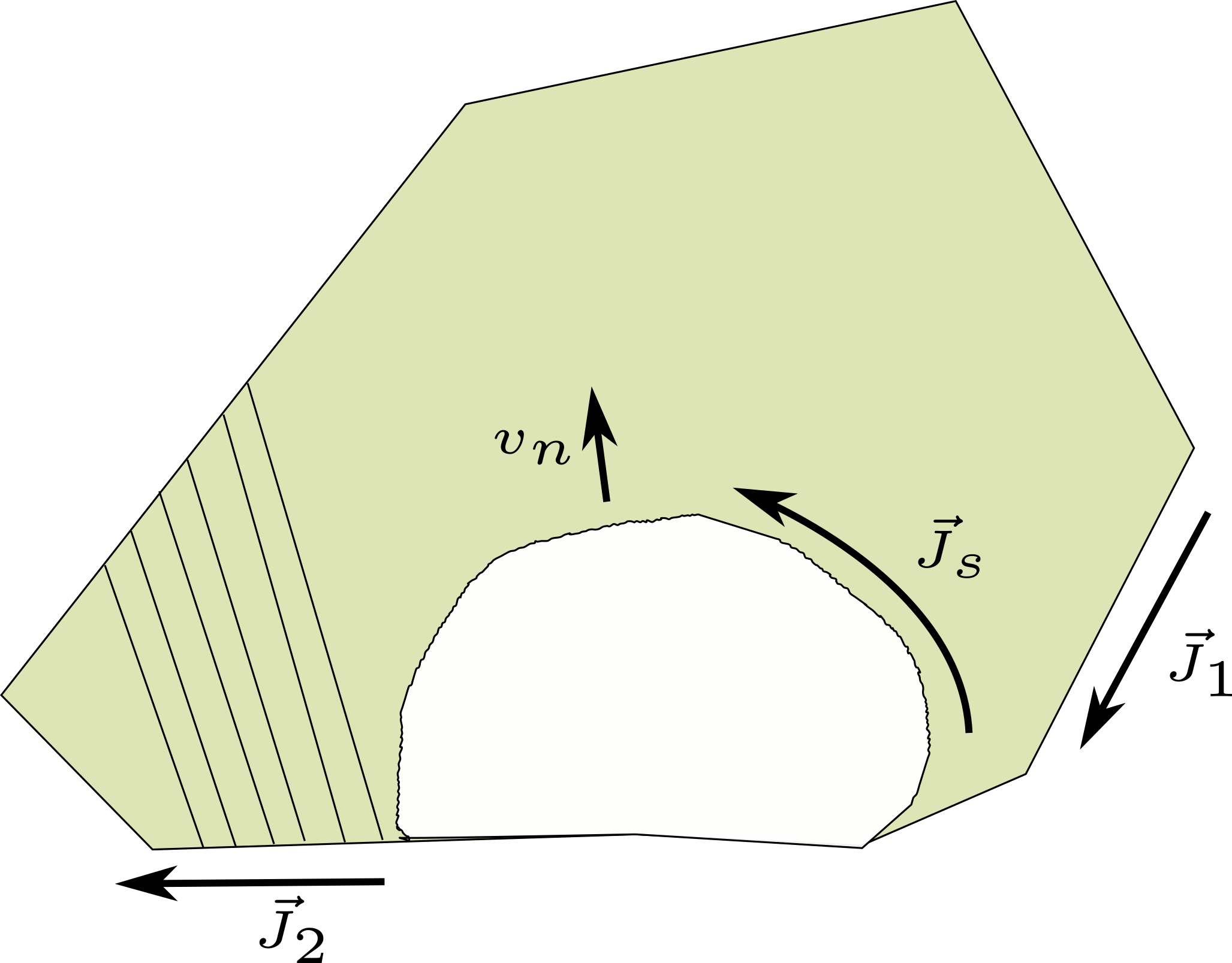
Fig. 2: Schematic representation of void growth inhibited by the presence of a nanotwin array.