
 |
|
||||
BiographyMohammad Davoudi received his bachelor's in Atomic and Molecular Physics from the Iran University of Science and Technology. He then started his master's in Particle Physics at Shahid Beheshti University where his research focused on Entanglement Entropy, Quantum Chromodynamics, and Gauge/Gravity duality (AdS/CFT). After graduation in 2019, he taught physics as a lecturer at the University of Eyvanakey. In June 2022 he joined the Institute for Microelectronics, working on novel semiconductors and insulators for the next generation of electronic devices, specifically FET transistors. |
|||||
Investigating the Quality of Insulating Layers as the Origin of Key Reliability Issues
While two-dimensional (2D) materials hold tremendous promise for future device technologies, as they are ideal for creating atomically thin channels to mitigate short channel effects, exhibit high theoretical mobilities, and offer the possibility to form hetero-structures or to realize short channel lengths, numerous challenges must be addressed to achieve the high performance, stability, and reliability necessary for industrial-scale application. The quality of the insulator slab and the insulator/semiconductor interface significantly influences the performance and reliability of field-effect transistors composed of these materials. Several critical reliability issues, including hysteresis, gate leakage current, random telegraph noise, and bias/temperature instability, stem directly from the insulating layer and can be investigated through phenomena such as charge trapping, trap-assisted tunneling, and ion diffusion in the insulating layer.
Hysteresis is a pervasive issue in these devices, characterized by a shift in the threshold voltage during up and down gate bias sweeps due to defects that trap and release charges. Various defects may arise in the device, primarily during the fabrication process. Investigating defects within the insulating layer provides a comprehensive understanding of this phenomenon, aiding in trap characterization and defect identification. This understanding is pivotal for discerning the dominant degradation mechanism in the device and devising preventive measures.
Conducting multi-faceted investigations, i.e., experimental characterization, DFT, TCAD, Compact model, etc., across different device structures is essential to better understand the intrinsic material properties. This approach helps distinguish measurement errors and one-time fabrication effects from potential major degradation mechanisms. Fig 1 illustrates the correlation between sweep frequency and observed hysteresis in a device fabricated from the promising high-mobility 2D material Bi2O2Se and its high-k native oxide Bi2SeO5 at two temperatures. Additionally, Fig 2 shows the schematics of finFET structures fabricated using the same material system.
In conclusion, addressing reliability issues in 2D material-based field-effect transistors requires a strong understanding of oxide layer quality and its impact on device performance. Through careful investigation of defects and degradation mechanisms, coupled with comprehensive analyses, progress can be made toward realizing the full potential of these innovative devices in future technologies.
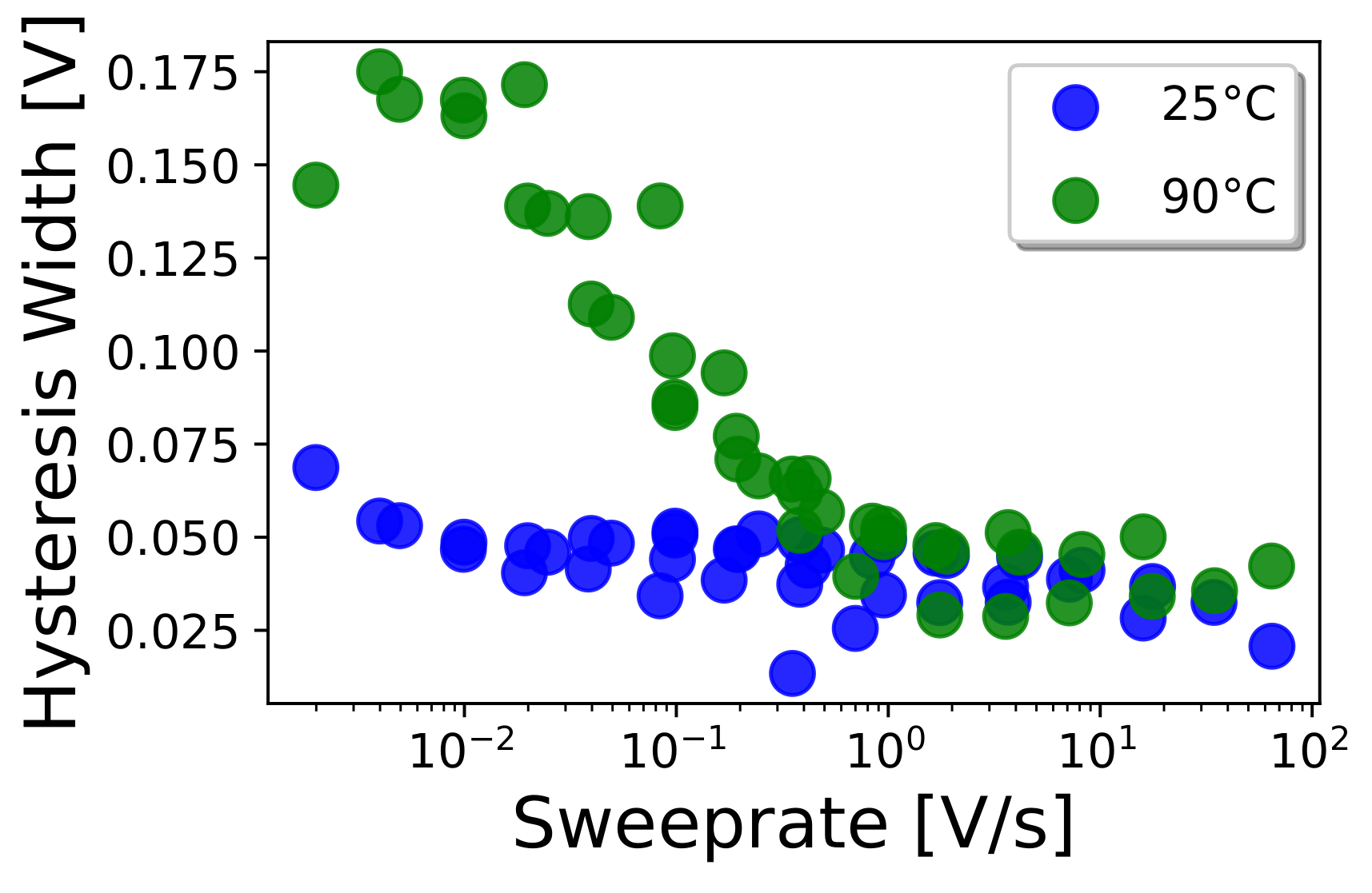
Fig. 1: Illustration of the correlation between sweep frequency and observed hysteresis in a device fabricated from the promising high-mobility 2D material Bi2O2Se and its high-k native oxide Bi2SeO5 at two temperatures.
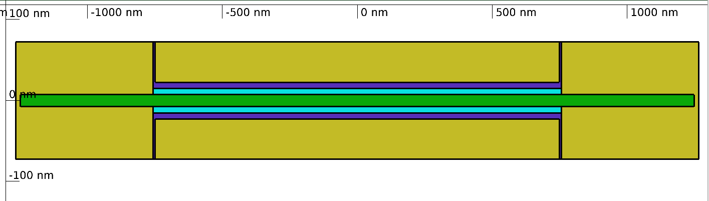
Fig. 2: The schematics of finFET structures fabricated using the same material system.