 |
|
||||
BiographyLado Filipovic is an Associate Professor and the Director of the Christian Doppler Laboratory for Multi-Scale Process Modeling of Semiconductor Devices and Sensors at the Institute for Microelectronics, TU Wien. Lado’s research is centered around Integrated Semiconductor Sensors and Process Technology Computer Aided Design (TCAD). He obtained his venia docendi (habilitation) in Semiconductor Based Integrated Sensors and his doctoral degree (Dr.techn.) in Microelectronics from TU Wien in 2020 and 2012, respectively. He holds a Master’s degree in Applied Sciences (MASc.) from Carleton University in Ottawa, Canada, which he obtained in 2009. Lado is currently heading several research projects from a wide range of technology readiness levels (TRLs) including basic research – funded by the Austrian Science Fund (FWF); applied research – funded by the Christian Doppler Forschungsgesellschaft (CDG), the Austrian Research Promotion Agency (FFG), and the European Union (EU); and industry research – funded by direct industry collaborations. He is a Senior Member of the IEEE and is an active member of the Technical Program Committee for many outstanding IEEE sponsored conferences. He has served as a reviewer for several European funding agencies, has edited two books on Miniaturized Transistors, and is an active reviewer for many leading journals. His research team has released several open-source scientific software tools under the ViennaTools moniker, such as the process simulator ViennaPS and the device simulator ViennaEMC, which have been applied for studying the fabrication and operation of advanced nanoelectronic devices. The research group currently collaborates with many industry partners (e.g., Silvaco, Infineon Technologies, Global TCAD Solutions, Fuji Electric) as well as academia from around the world (e.g., MIT, Arizona State University, University of Glasgow, University of Groningen, University of Vienna, Chinese Academy of Sciences). Lado's primary research interest is studying the operation, stability, and reliability of novel semiconductor-based sensors using advanced process and device simulations. An additional pillar of his research is the multi-scale modeling of processes involved in the fabrication of semiconductor devices and sensors. This involves combining atomistic modeling with Monte Carlo and continuum approaches, as well as merging physical and empirical modeling in a single framework, specifically in process TCAD. He is also actively investigating metal oxide semiconductors and novel two-dimensional (2D) materials, e.g., graphene, MoS2, and phosphorene for the detection of biomarkers and environmental pollutants. In particular, his group is investigating the impact of the adsorption of ambient gas molecules on the surfaces of 2D semiconducting films and on the performance of devices and sensors based on these. Software Development:Process Simulator ViennaPS Research Topics:Semiconductor Sensors Running Public Projects:FWF - Adsorbate-Dependent Conductivity of MoS2 CDG - CDL for Multi-Scale Process Modeling of Semiconductor Devices and Sensors |
|||||
Green Technology Development with Machine Learning Supported Process TCAD
Over the last few decades, planar transistor scaling at advanced technology nodes has been replaced by complete transistor redesign and the introduction of new materials and fabrication steps. The main reason is the limited control over the channel region offered by the planar design. Therefore, transistor geometries have gone vertical, first with the FinFET structure and now with the gate-all-around (GAA) field effect transistor (FET). This trend has added significant complexity to the design of novel technology nodes, meaning that more time and money is invested in investigating novel materials, advanced processes, and equipment limitations and variability. For this, semiconductor manufacturers fabricate many experimental wafers to test each process and to understand its limitations. However, the fabrication of experimental wafers takes significant time and the operation of expensive cleanroom resources. In addition, the equipment requires high power consumption and can produce highly polluting byproducts, which contribute to pollution and increase the overall CO2 footprint of the semiconductor industry. Therefore, creating an accurate digital twin of the fabrication equipment would reduce the time, cost, and CO2 footprint of every design cycle.
One of the main limitations of the current approach for process technology computer-aided design (TCAD) is that most models provide a qualitative link to measurements and require significant calibration to represent real devices and structures. In addition, the inputs or parameters required by feature-scale models, typically provided by process TCAD tools, are detached from the equipment settings. This is because equipment-level simulations require length scales on the order of tens of centimeters, referred to as reactor-scale simulations. In contrast, feature-scale simulations are on the order of several nanometers or micrometers. The multi-scale approach to simulating the combined effects typically involves performing full reactor-scale simulations, extracting the near-wafer fluxes from these simulations, and then applying those to feature-scale models. However, this method still requires heavy calibration to realize a complete link with cleanroom equipment for these models.
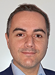
We are working on a simulation framework combining physics-based etching and deposition models with equipment inputs. The idea behind the approach is provided in Figure 1, where the outputs of equipment simulations or experiments are used to train a machine learning model, which is directly applied to a process TCAD framework, ViennaPS, which we are also developing in our research group. The machine learning (ML) model can be trained on neutral radical and ion fluxes for physical modeling or geometric descriptors for process emulation. Process emulation can be particularly useful when designing the next technology node to assess the limitations in pitch or critical dimensions that a particular process can obtain.
As a first step, we have implemented an etching model in a dry SF6/O2 inductively coupled plasma (ICP). We have calibrated a physical model based on experimental measurements. However, this model requires knowing the fluxes of several species, such as the chemical etchant F, passivating species O, and sputtering ions, immediately above the wafer surface. Using Gaussian process regression (GPR), we train an ML model to provide the required top-of-wafer fluxes based on equipment inputs, such as the gas flow rates of SF6 and O2, the chamber pressure, the ICP power, the platen power, and the temperature. By combining the GPR model with ViennaPS, we can provide a physical plasma etching model that takes chamber settings and the initial wafer geometry as inputs and provides the final etched profile as an output. Two examples of different process conditions are provided in Figure 2.
As we continue to add more models to our library, we can merge our physical models with equipment knowledge. Working together with process engineers, this approach will significantly reduce the time and money spent fabricating experimental wafers. The added benefit will be the reduced need to use power-hungry and environmentally unfriendly equipment, helping to usher in a green revolution in semiconductor fabrication.
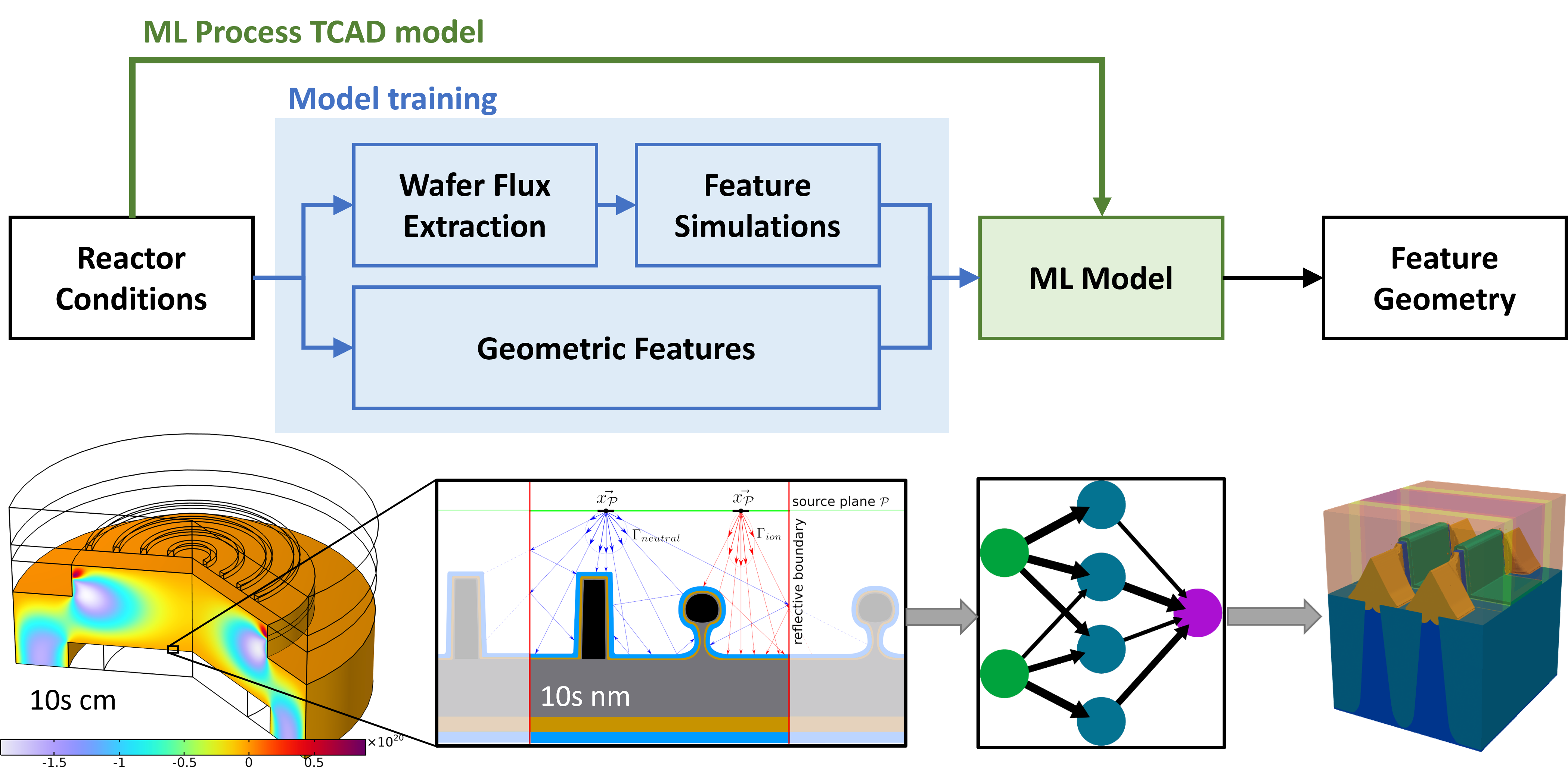
Fig. 1: Training a multi-scale machine learning-based process model includes combining chamber simulations or measurements with feature scale physical simulations or geometric emulations.
Fig. 2: Results of etching through a cylindrical mask with diameter 40μm, thickness 20μm, and 2o tapering in an SF6/O2 plasma with an ICP power of 800W and temperature of 5oC. The SF6 flow, O2 flow, pressure, and platen power are (left) 80sccm, 0sccm, 5mTorr, -40V; (middle) 72sccm, 8sccm, 40mTorr, -40V; (right) 40sccm, 40sccm, 25mTorr, -80V.