
 |
|
||||
BiographyAlexander Karl rreceived his Bachelor and Master degrees in Technical Physics from TU Wien in 2020 and 2022, respectively. For his Master's thesis he focused on the search for Dark Matter with the CRESST experiment. In August 2022 he joined the Institute of Microelectronics and is pursuing his PhD studies. Currently, his research is focused on the modeling of 2D field effect transistors using, e.g., the compact physics framework Comphy, and on investigating the application of novel 2D materials towards the realization of electronic devices. |
|||||
Investigating the Hysteresis in the Transfer Characteristics of 2D-MOSFETs
Metal-oxide-semiconductor field-effect Transistors (MOSFETs) continue to play the leading role in shaping the performance and functionality of integrated circuits. With the rapid advancement of materials science, integrating two-dimensional (2D) materials, such as transition metal dichalcogenides (TMDs), has emerged as a promising approach to push the performance boundaries of MOSFETs. The atomically thin nature of 2D materials is an enormous advantage for device scaling, allowing for the creation of smaller and more efficient MOSFETs. Despite the promising attributes of this new material class, currently available prototype MOSFETs based on two-dimensional materials (2D-MOSFETs) are susceptible to environmental conditions, often displaying poor stability and reliability. To unlock the full potential of 2D-MOSFETs for future electronic applications, it is necessary to understand the physical mechanisms contributing to these instabilities.
Therefore, we investigate the instabilities of the transfer characteristics of 2D-MOSFETs. For this purpose, we have developed a comprehensive compact model for the drain current of 2D-MOSFETs, considering the impact of interface defects, oxide charges, and ohmic contact resistances. To validate our proposed compact model, we have analyzed the bottom-gated 2D-MOSFET depicted in Fig. 1, which comprises a p++ doped Si gate, a SiO2 oxide, and an MoS2 channel. Fig. 2 illustrates the measured Id-Vg curves alongside the predictions generated by our compact model. Circles represent the experimental data, while solid lines depict the simulations. Our model demonstrates excellent agreement with experimental data across various operating conditions.
Considering time-dependent phenomena such as charge trapping, mobile ion drift, and ferroelectrics, the threshold voltage of the transistor may experience shifts. As a result, the Id-Vg curve recorded when turning the device on may not match the curve recorded when turning the device off, leading to Hysteresis in the transfer characteristics. This shift in the threshold voltage is a characteristic measure of the stability of the device and is referred to as the hysteresis width. Fig. 3 depicts the hysteresis width of the device under investigation alongside our compact model's predictions. The positive Hysteresis observed at 22°C is attributed to charge trapping near the channel interface, while the negative Hysteresis at 165°C is linked to the drift of mobile ions in the oxide layer. By considering these mechanisms, the device's Hysteresis can be accurately modeled across a broad frequency and temperature range. This analysis underscores the importance of hysteresis measurements and a comprehensive hysteresis model as effective tools for identifying the underlying physical mechanisms of reliability issues.
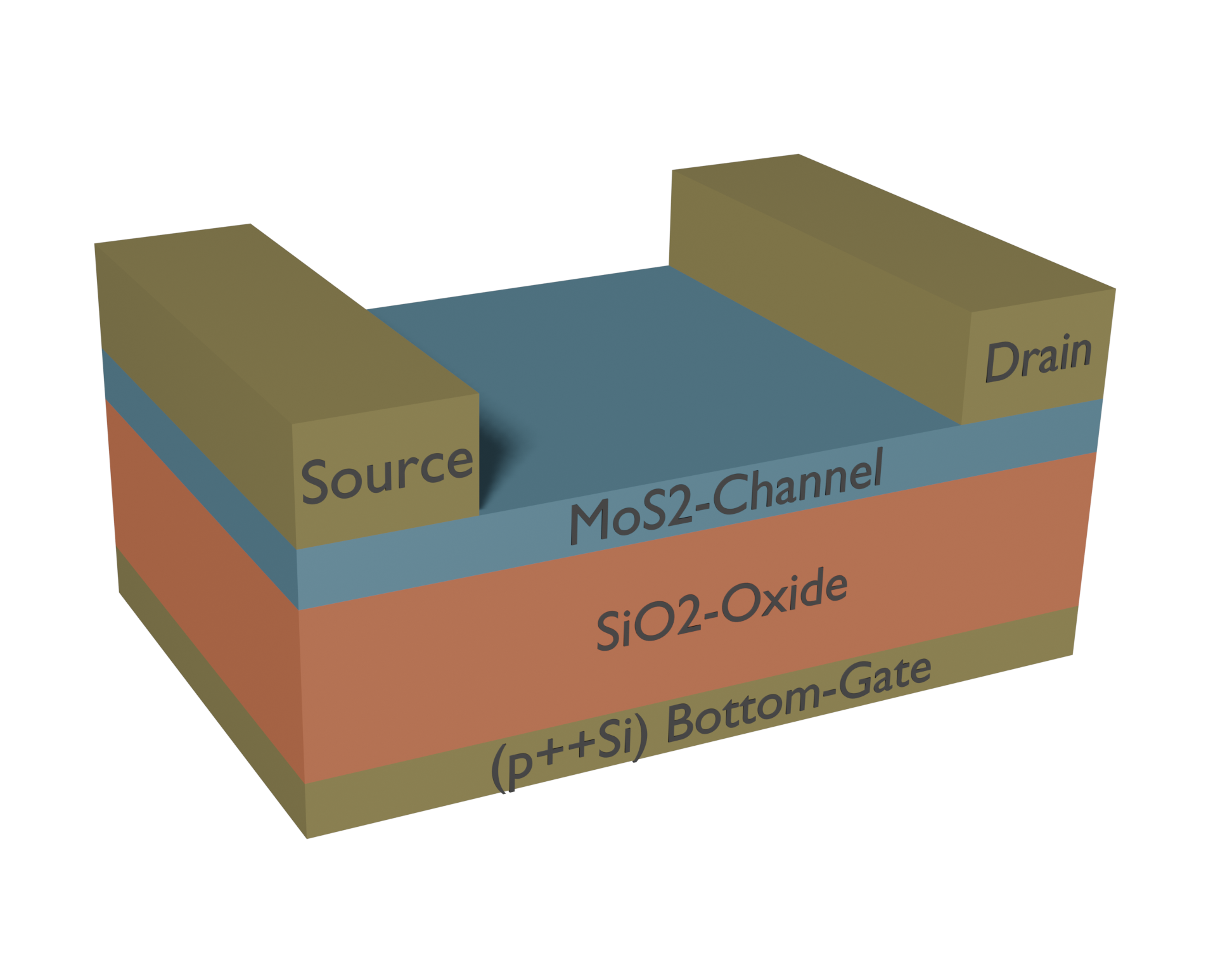
Fig. 1: Structure of the 2D-MOSFET under investigation. The device consists of a p++ doped Si gate, a SiO2 oxide, and an MoS2 channel.
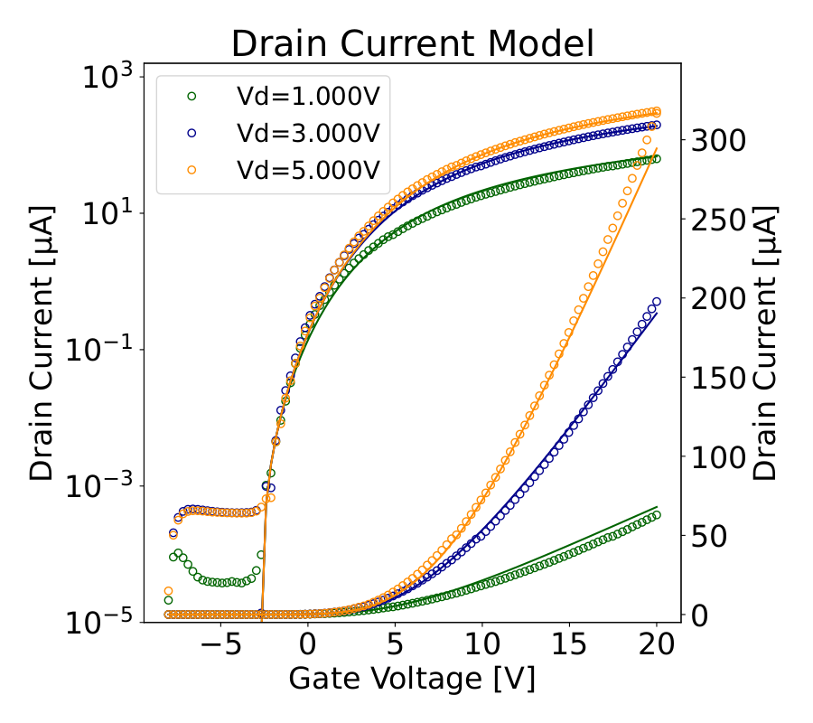
Fig. 2: Comparison of experimental Id-Vg curves and the calibrated compact model for the p++\Si\SiO2\MoS2 device. The circles represent the experimental data, and the solid lines represent the simulation. The simulation took into account the effect of fast interface defects, fixed oxide charges, and ohmic contact resistances.
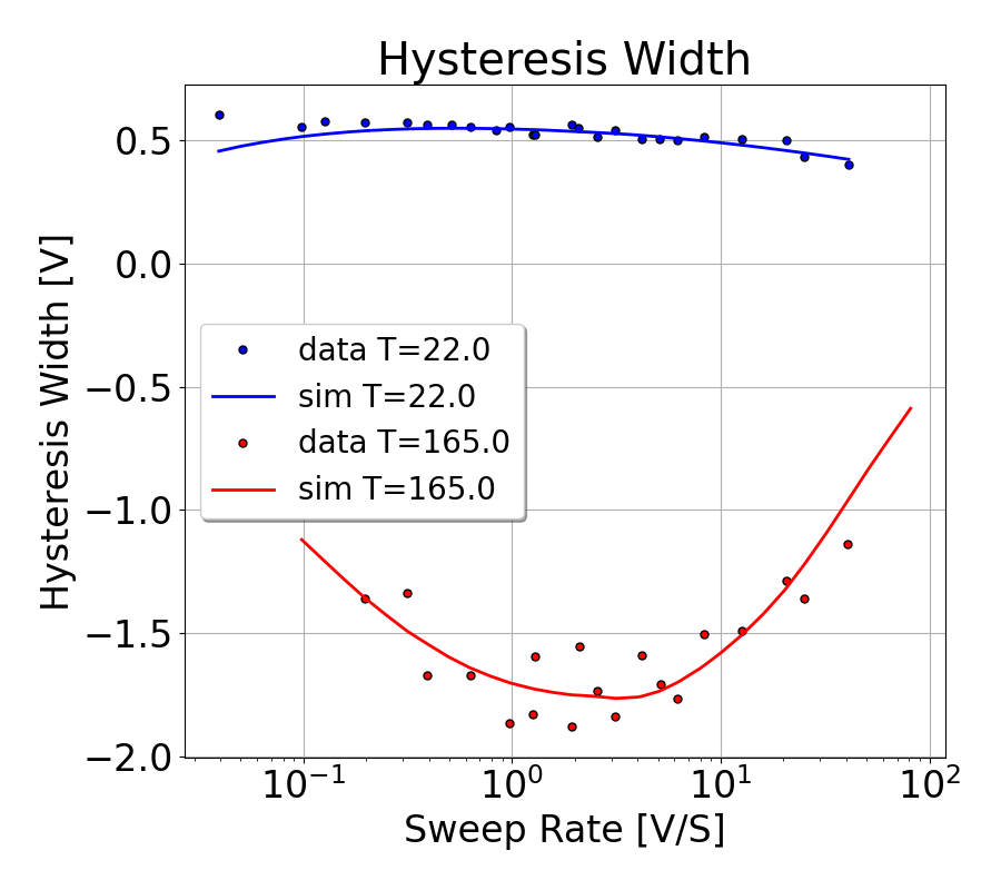
Fig. 3: Comparison of experimental hysteresis curves and calibrated compact model for the p++Si/SiO2/MoS2 device. The dots represent the experimental data, and the solid line represents the simulation. The clockwise Hysteresis at 22°C was attributed to charge trapping due to oxide defects near the channel interface, and the counterclockwise Hysteresis at 165°C was modeled by placing mobile ions in the oxide.