
 |
|
||||
BiographyTheresia Knobloch is a postdoctoral researcher focusing on fabrication, experimental characterization, and physical modeling of nanoelectronic devices based on 2D materials. She obtained her doctoral degree from TU Wien in 2021 and performed parts of her Ph.D. research as a visiting scholar at Purdue University, USA in 2018 and 2019 and Soochow University, China in 2017. For her work, she received several awards including the IEEE EDS Ph.D. Student Fellowship in 2021 and the Best Student Paper Award at the DRC in 2020. She joined the Institue for Microelectronics in 2016 while completing her master's degree in microelectronics and photonics. She acquired both her M.Sc. in 2016 and her B.Sc. in technical physics in 2014 from TU Wien with distinction. Currently, she primarily studies the electrical stability and reliability of 2D material-based field-effect transistors. |
|||||
Modeling the Reliability of Field-Effect Transistors Based on Two-Dimensional Semiconductors
Two-dimensional (2D) semiconductors offer the potential for highly miniaturized field-effect transistors (FETs) with gate lengths below 12 nm. Towards this goal, the channel thickness must also be scaled down, typically following a relationship where the thickness is proportional to one-fourth of the gate length. Thin silicon sheets with thicknesses below 5 nm suffer from degraded mobility due to increased carrier scattering at the interfaces, while 2D semiconductors, being only a few atoms thick, maintain good carrier mobilities. For instance, molybdenum disulfide (MoS2) exhibits an electron mobility of up to 120 cm2V-1s-1, while layered bismuth oxyselenide (Bi2O2Se) boasts a high carrier mobility of up to 500 cm2V-1s-1. Consequently, according to the International Roadmap for Devices and Systems, 2D semiconductors are considered potential channel materials for technology nodes beyond 2034. However, before the industry can utilize 2D semiconductors commercially, the research community must address several challenges.
Current 2D FETs must transition from lab-scale prototypes to large-scale fabrication, necessitating predictive physical modeling tools. Transport models, ranging from moderate to high physical accuracy, must be developed, with computational costs increasing as accuracy rises. Efficient modeling tools such as the technology computer-aided design (TCAD) implementation of drift-diffusion (DD) equations are preferred for describing experimental 2D FETs with large device dimensions in the micrometer regime. Moreover, a computationally efficient model is essential for combining transport descriptions with models for the impact of defects, addressing the critical challenge of ensuring reliable operation throughout the device's lifetime. One significant challenge for 2D FETs is the lack of suitable gate insulators, leading to high densities of interface and border traps that cause the observed hysteresis, bias temperature instability, and low-frequency noise. We have employed the non-radiative multiphonon model to simulate the transfer of charge to point defects at the interface or within the oxide, enabling the description of both device performance and reliability. In Figure 1, a schematic cross-section through an experimental bismuth oxyselenide FET prototype is shown, where its native oxide, bismuth selenium oxide (Bi2SeO5), is used as a top gate oxide. We used a combination of DD TCAD and the non-radiative multiphonon model to describe the observed clockwise hysteresis in the transfer characteristics of these Bi2O2Se FETs, as shown in Figure 2.
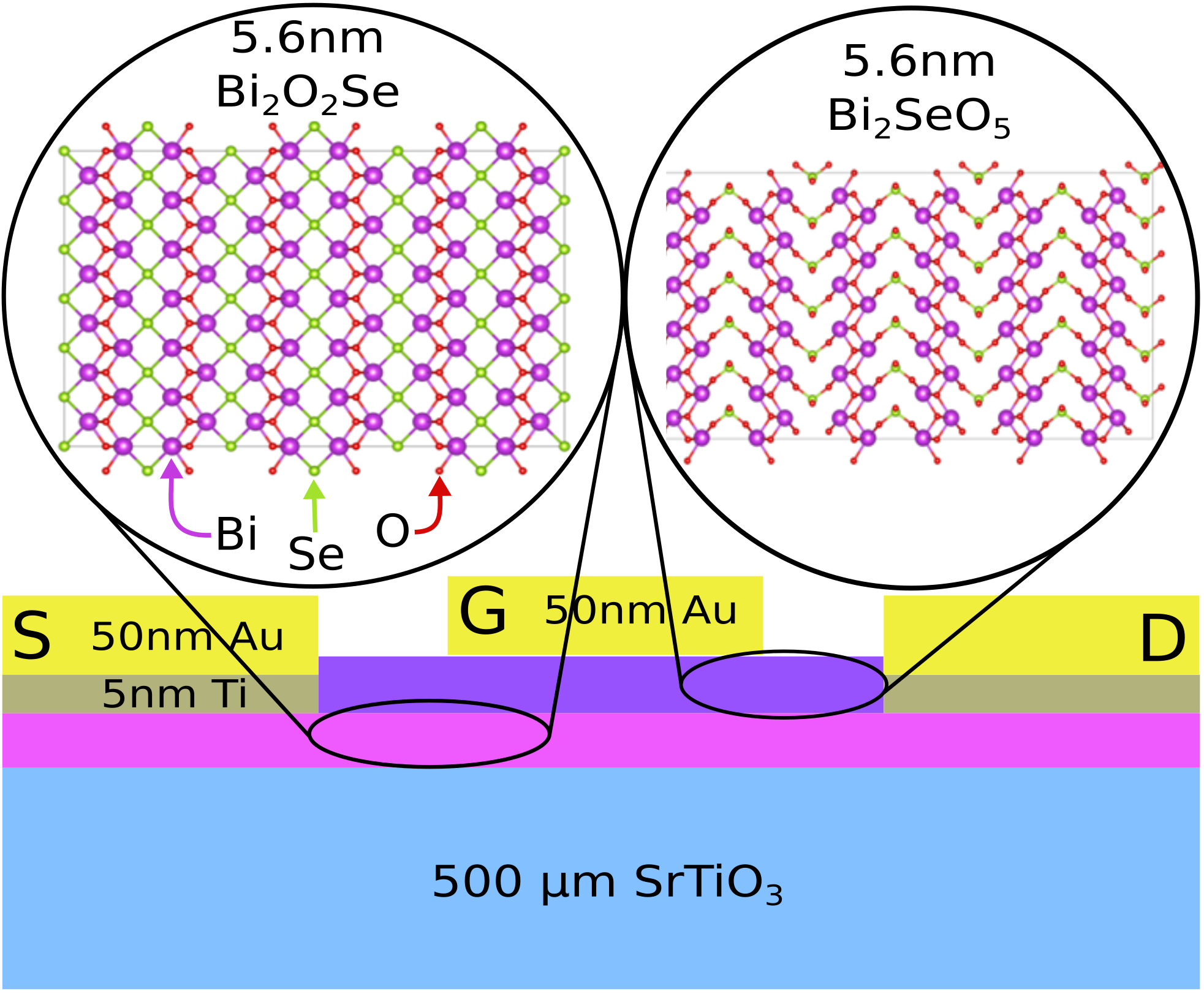
Fig. 1: Schematic drawing of the cross-section through a Bi2O2Se / Bi2SeO5 2D FET.
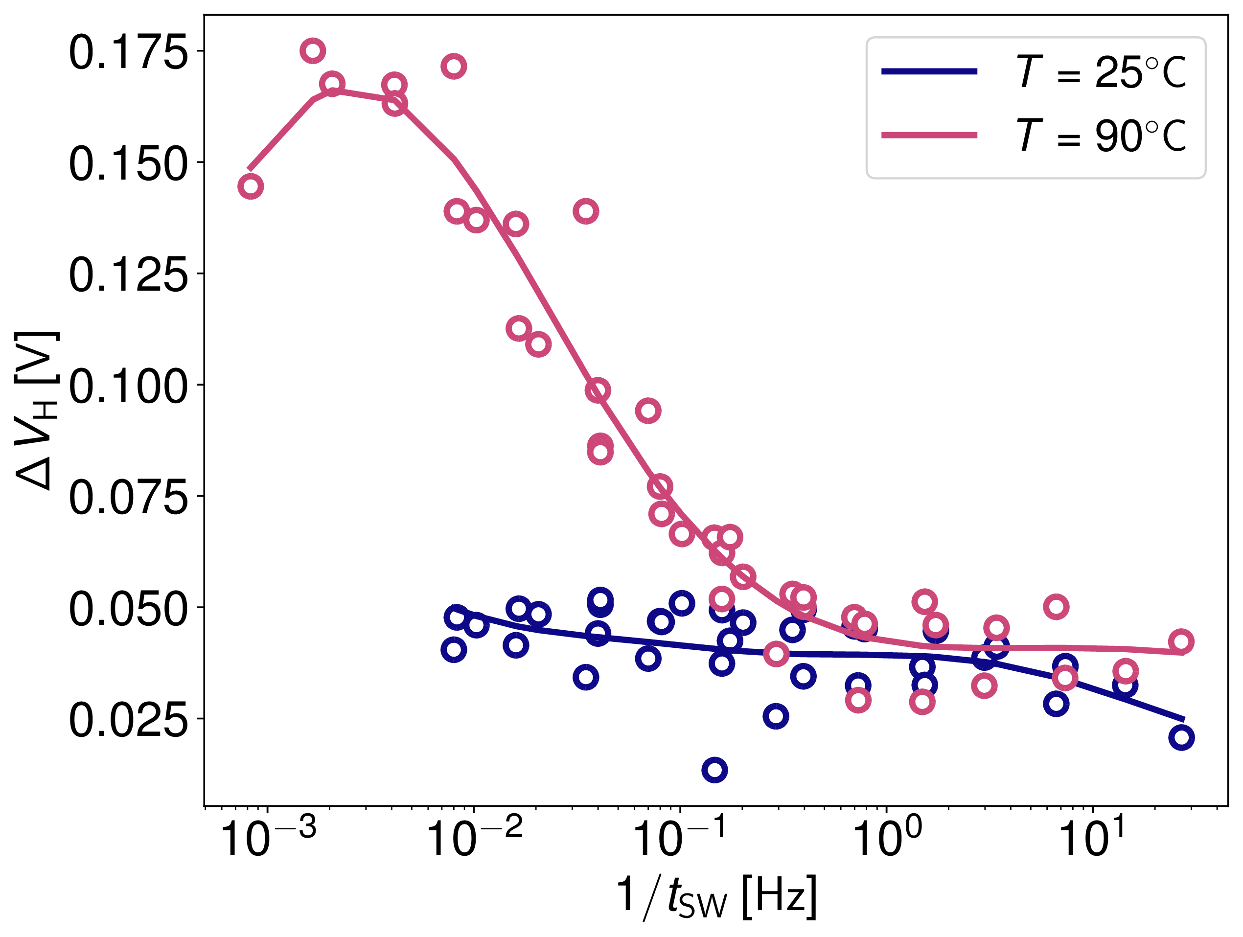
Fig. 2: A clockwise hysteresis in the transfer characteristics is observed at two different temperatures for Bi2SeO5 2D FETs. The DD TCAD model coupled to a non-radiative multiphonon model (lines) agrees well with the measurement data (circles).