
 |
|
||||
BiographyDavid Lamprecht was born in South Tyrol, Italy, and received both his Bachelor and Master’s degrees in Physics at the University of Vienna in the Physics of Nanostructured Materials (pnm) Group of Prof. Jani Kotakoski. David joined the Institute for Microelectronics in June of 2023, where he is pursuing a PhD degree with a focus on understanding the impact of the adsorption of ambient gas molecules on the surfaces of 2D semiconducting films and on the performance of devices and sensors based on these. He works in close cooperation with his former group and uses the Nion Ultra-STEM 100 scanning-transmission electron microscope located at Sternwarte Park, Vienna to characterize 2D materials like Mos2. |
|||||
Atom-Level Substitutional Doping of MoS2 Monolayers
State-of-the-art semiconducting metal oxide (SMO) gas sensors require elevated temperatures and large microheaters, leading to mechanical instability, limited lifetime, high costs, and incompatibility with complementary metal-oxide-semiconductor (CMOS) fabrication. Semiconducting two-dimensional (2D) materials, especially transition-metal dichalcogenides (TMDs) like MoS2 and WS2 are a promising alternative to SMO gas sensors: Their high surface-to-volume ratio ensures high sensitivity to ambient molecules, even at low temperatures, and the relatively facile synthesis by chemical vapor deposition (CVD) shows potential for CMOS integration.
One large obstacle in the course toward TMD-based devices is the low carrier mobility of the pristine form of these materials, which has major consequences for the gas response, selectivity, and response time of TMD-based devices and sensors. To address this issue, we utilize the various manipulation methods and characterization techniques of the ultra-high-vacuum (UHV) system at the Sternwarte laboratory to change significant material properties of the CVD-grown MoS2 monolayer. Low-energy helium ions stemming from a plasma source are used to introduce controlled defects in MoS2 (see Figure 1). Subsequently, the defect sites are filled with desired heteroatoms (e.g., Au, Pt) via e-beam evaporation of metal target rods. The resulting structures are characterized via aberration-corrected scanning-electron-microscopy (SEM). The incorporation of dopant atoms is investigated by combined atomic-scale HAADF imaging and electron-energy-loss spectroscopy. We have identified the plasma settings that can reliably produce molybdenum mono-vacancies and successfully implanted Ag dopants into the MoS2 lattice. In future experiments, we aim to increase the density of the dopants and implant other elements into our lattices. Once suitable samples have been produced, the gas sensing properties of the material will be tested using our specially designed gas sensor wafer prober.
Additionally, we focus our research on the interaction between 2D materials and airborne contaminants. Even a small concentration of hydrocarbons can impede certain material modification methods like low energy ion irradiation or change the properties of the 2D material under test. We have attempted various cleaning methods, such as in-situ laser annealing, and were able to produce μm sized clean sample areas, which remained stable for several hours in ultra-high-vacuum. Future research will examine the interaction between hydrocarbon contamination and active sites in the material and explore its influence on gas adsorption properties.
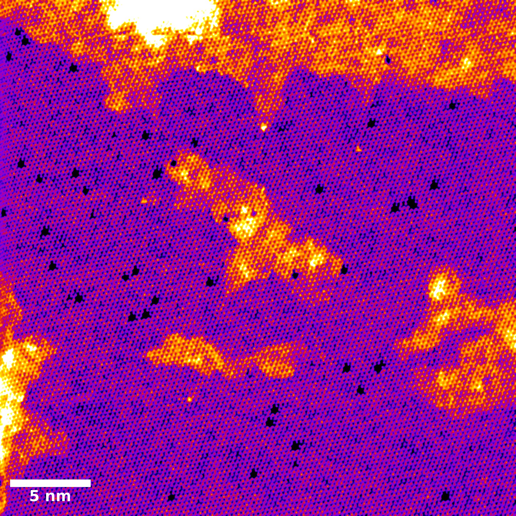
Fig. 1: 60 kV HAADF STEM picture of a Mos2 monolayer after low-energy helium ion irradiation. The large triangular features are molybdenum monovacancies surrounded by sulfur defects. The smaller features are sulfur mono- and double vacancies. Orange colored areas are covered by hydrocarbon contamination.