
 |
|
||||
BiographySeyedmahdi Sattari-Esfahlan received his Master's degree in Photonics and Nanoelectronics from the University of Tabriz, Iran in 2016 and his Doctorate in Electronic Engineering from the Seoul National University/Gachon University, South Korea in 2022. During his PhD his main research focus was on advanced material science, nanoelectronic devices, and neuromorphic computing. As a postdoctoral fellow, he joined the Institute for Microelectronics at TU Wien in August 2022. Currently, Dr. Sattari-Esfahlan is working on the device fabrication and characterization of 2D-material-based electronic devices with different gate insulators, analyzing the performance and reliability of 2D FETs. |
|||||
Fabrication and Reliability Characterization of High-k 2D FET Devices
Two-dimensional (2D) field-effect transistors (FETs) demand scalable gate dielectrics to deliver their full theoretical performance potential. The universal properties of the gate dielectric and its interface with the 2D channel are key factors determining the performance of 2D FET devices and the degradation of device performance, rooted in the implemented insulator properties. The fundamental properties of relevance for high-performance gate dielectric are permittivity, band gap, thermodynamic stability, band alignment, interface quality, and process compatibility with CMOS technology. High-k dielectrics provide a significant increase in physical thickness, resulting in reduced leakage and enhanced gate capacitance. They are primarily compatible insulators demonstrating high promise for application in 2D FETs via van der Waals binding to the 2D semiconducting channel. Many high-k dielectrics overcome the charged impurity scattering, exhibiting higher mobility in 2D/dielectrics devices than many other insulators. Nanometer-thick CaF2, SrTiO3, and Bi2SeO5 are among many other high-k insulators that showed a very low defect density (responsible for hysteresis and long-term drifts of the device performance) and significantly fewer leakage currents even at higher operating temperatures. However, from the technological point of view, it is critical to understand the insulators' long-term stability and reliability properly. Thus, along with device fabrication, our research mainly focuses on transfer characteristics, hysteresis, and bias temperature instability (BTI) behavior of fabricated 2D FETs at cryogenic, room, and high temperatures. The reliability performance of a variety of promising high-k dielectrics have been studied, such as SrTiO3, MnAl2S4, Bi2SeO5 (Fin-FET), Sb2O3, and boron nitride (encapsulated FET). Subsequently, the work involves proposing possible solutions such as the realization of clean interfaces using van der Waals binding between the 2D-channel and the high-k insulators, analyzing the interface quality by electron microscopy and X-ray spectroscopy approaches, and studying reliability performance based on single defect spectroscopy. Finally, our high-k 2D FETs demonstrated elevated device performance, such as a high On/Off ratio, small threshold voltage, and very low leakage current. Also, devices showed low hysteresis width even at high temperatures with small threshold voltage shifts (PBTI degradation), as shown in the figure. Therefore, high-k materials investigated here are among the most promising gate dielectrics for next-generation ultra-thin nanoelectronics.
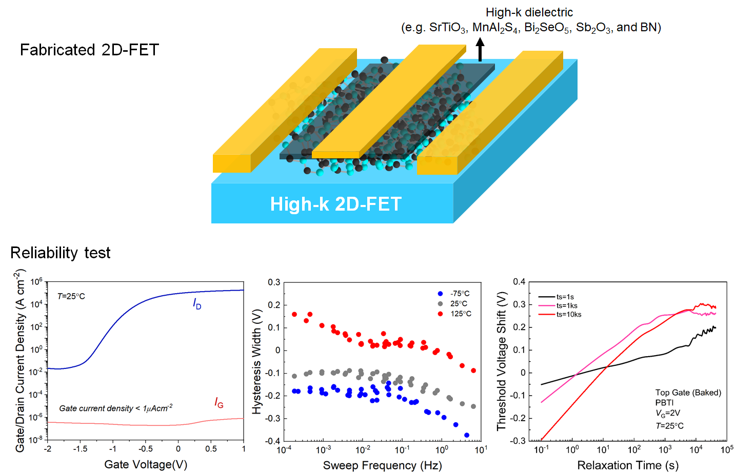
Fig. 1: (top) Schematic diagram of fabricated 2D FET with different high-k gate dielectrics. (bottom) reliability test, including transfer curve and gate leakage current (left), hysteresis width curve over sweeping frequency (middle), and PBTI curve at different stress periods over recovery time (right).