 |
|
||||
BiographyIgor Sokolović is a postdoctoral researcher focused on the design and the construction of prototype next-generation nanoelectronic devices. He obtained his PhD degree for the experimental and theoretical research of complex oxide surfaces in the field of Surface Physics at the Institute of Applied Physics at the Technische Universität Wien in 2021, following his undergraduate and graduate studies in the Solid State Theoretical Physics at the University of Novi Sad. His expertise lies in the microscopy and spectroscopy of surfaces at the atomic level in ultra high vacuum. This well- controlled environment leads to the growth and characterization of devices based on 2D semiconductors and insulators, capable of surpassing the quantum limit. |
|||||
Growth of CaF2 on Metal Supports and the Search for Alternative Dielectrics
To overcome the challenges of current field-effect transistor (FET) technology, we search for dielectrics as an alternative to SiO2 that would prevent tunneling through a thin gate insulator (~3 nm) while providing sufficient coupling to the underlying active channel of a FET. In the previous year, we underwent two different pathways in this direction.
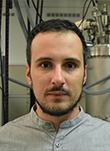
First, we investigate the potential of the CaF2 fluoride salt as a next-generation dielectric material by growing it on different substrates. For growth, we employ a molecular-beam epitaxy (MBE) method in ultra-high vacuum (UHV) on atomically clean substrates, while for characterization, we employ in-situ low-energy electron diffraction (LEED) and Auger electron microscopy (AES) and ex-situ ambient atomic force microscopy (AFM). We studied the growth of CaF2 on elemental Cu single crystals with different surface orientations to understand the growth mechanism at the fundamental level; some results are provided in Figure 1.
CaF2 films were found to grow by exposing the (111) face on both Cu(110) and Cu(111). At elevated substrate temperatures, where the diffusion of CaF2 molecules to assume a minimum energy configuration is permitted, we observe disconnected islands of CaF2(111). This indicates that this dielectric's very low surface energy must be considered when attempting growth on other promising materials. To overcome this, we achieved the growth of amorphous CaF2 films under certain conditions, and we will explore this further.
Second, we investigate alternative dielectrics. In the past year, we collaborated with Prof. Zdenek Sofer from UTC Prague and focused on a novel LaOBr insulator with a dielectric constant of approximately 9 and a band gap of 5.3 eV. The small size of these flakes hinders their use in widely employed surface characterization techniques, so we employed non-contact atomic force microscopy (ncAFM) in UHV to observe the pristine LaOBr lattice with atomic resolution and characterize the intrinsic atomic-scale defects, seen in Figure 2. Such characterization enables us to understand the behavior of future devices. We aim to construct devices using LaOBr and investigate other oxybromine, oxychlorine, and oxyiodine dielectrics.
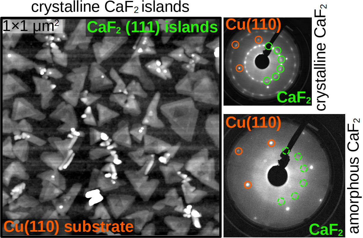
Fig. 1: Cu(110) surface covered with a 0.8 nm thick CaF2(111) film. Tapping mode AFM (left panel) shows that the film is reorganized in disconnected islands of two-unit-cell-thick CaF2. LEED pattern displays clear Cu(110) and CaF2 diffraction spots. The bottom-right panel shows a LEED pattern of the same substrate covered with a 0.3 nm thick amorphous CaF2 film: the substrate spots are clearly visible while the CaF2 are ill-defined.
Fig. 2: LaOBr single crystals (synthesized by Prof. Zdenek Sofer) studied at the atomic level using ncAFM. The left panel shows a pristine lattice of Br atoms terminating a cleaved or exfoliated surface; the right panel shows the appearance of intrinsic defects in the lattice (marked in red), currently interpreted as Mg impurities substituting bulk La atoms.