 |
|
||||
BiographyBernhard Stampfer, born in 1989 in Austria, studied at the Technische Universität Wien where he received the Bachelor’s degree (BSc) in Electrical Engineering (2013), the Diplomingenieur degree (Dipl.-Ing., MSc equivalent) in Microelectronics and Photonics (2016) and the Doctoral degree (Dr.techn., PhD equivalent) in 2020. Bernhard is employed at the Institute for Microelectronics as a post-doctoral researcher and his work is focused on the characterization of defects in semiconductor devices. |
|||||
Developing Specialized Measurement Equipment for Semiconductor Reliability Studies
We regularly perform specialized characterization schemes to probe phenomena such as random telegraph noise (RTN), hysteresis, or bias-temperature instability (BTI) to study the performance and reliability of semiconductor devices and material systems. We typically study field effect transistors (FETs) or diodes using novel two-dimensional (2D) materials.
While such characterizations are often possible using commercially available measurement equipment such as source measure units and storage oscilloscopes, custom measurement equipment, tailored specifically to the task at hand, usually allows for a more comprehensive characterization range or improved measurement resolution, thus yielding more valuable results. While versatile, commercial instruments often lack the flexibility to tailor measurement configurations to our specific needs.
To give some examples, source measure units, while very flexible, are often limited in sampling rate and buffer depth, which restricts the characterization range for RTN measurements. For hysteresis and BTI measurements, these measure units might also limit repetitions or cause detrimental delays between measurement or preconditioning phases. While storage oscilloscopes can sample very quickly, they often lack the required y-resolution, meaning they must be paired with a function generator and transimpedance amplifier, which introduces additional complexity while often limiting flexibility in measurement schemes.
For these reasons, at the Institute for Microelectronics, we have developed a flexible measurement system that can be set up and programmed specifically for the measurement task at hand, with parameters tailored to the technology under investigation. A schematic overview of the measurement system, configured for FET measurements, is shown in Figure 1. Note that the number and type of units in the system can be customized, and each is programmable individually, resulting in significant flexibility. By continuously improving our system's capabilities, we can use new measurement schemes and learn about the advantages and challenges of novel material systems.
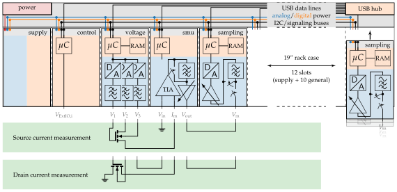
Fig. 1: Schematic overview of the measurement system developed at our institute. Analog and digital blocks are given in blue and orange, respectively.