
 |
|
||||
BiographyDominic Waldhör was born in Linz, Austria in 1992. He studied at the TU Wien, Vienna, Austria where he received the BSc degree in Electrical Engineering and the Diplomingenieur degree in Microelectronics and Photonics in 2018. He joined the Institute for Microelectronics in October 2018 where he works as PhD student. His current research focuses on the ab initio simulation of oxide defects in semiconductor devices. |
|||||
Identifying Defects in Charge Trapping Related Phenomena
Charge trapping phenomena at oxide defects in nanoelectronic devices influence device reliability through effects such as bias temperature instability (BTI), trap-assisted tunneling (TAT), and random telegraph noise (RTN). These problems persist on macroscopic and quantum scales, highlighting the urgency to understand the microscopic processes leading to device degradation. Our research aims to identify the defects at the semiconductor/oxide interface responsible for this degradation by combining experimental characterization techniques with a multiscale modeling approach. While the behavior of individual defects is studied theoretically with atomistic first-principles calculations, the impact of these defects on the device scale can be understood using a device model.
For device modeling, we employ our recently published and publicly available compact device simulator Comphy v3.2, which consists of a 1-dimensional electrostatic model of the device combined with a physical description of charge trapping dynamics at defects using the nonradiative multiphonon (NMP) model. In this model, the defect is characterized by two key parameters: the thermodynamic trap level ET and the relaxation energy ER. With Comphy, the distribution of these parameters can be extracted semi-automatically from experimental data, serving as a “fingerprint” of the defects. To identify defects based on this fingerprint, parameters can be predicted from first principles using Density Functional Theory (DFT) for any given defect candidate. This requires an atomistic model of the amorphous gate oxide, as shown in Fig. 1 (left). A melt-quench procedure within a classical molecular dynamics simulation can create such a model. However, the credibility of the resulting structure must be verified against experimental data, such as the structure factor from neutron diffraction, as shown in Fig. 1 (right).
With this methodology, we provide a robust tool for identifying defects based on relatively simple electrical measurements that can be conducted on fully processed devices. As an exemplary use case of our framework, we analyzed RTN signals on cryo-CMOS devices for future quantum applications. We extracted the corresponding capture and emission time constants, as shown in Fig. 2 (top). Based on these time constants' temperature and bias dependence, we determined the parameters of the underlying defects causing the noise. As shown in Fig. 2 (bottom), the resulting parameters are inconsistent with previously extracted defects in amorphous SiO2. However, they agree well with interface defects such as the classical Pb center, demonstrating that these interface defects play a crucial role in causing noise at cryogenic temperatures.
Further details and applications of our workflow can be found in the corresponding publication:
D. Waldhoer et al., Microelectronics Reliability 146, 115004 (2023)
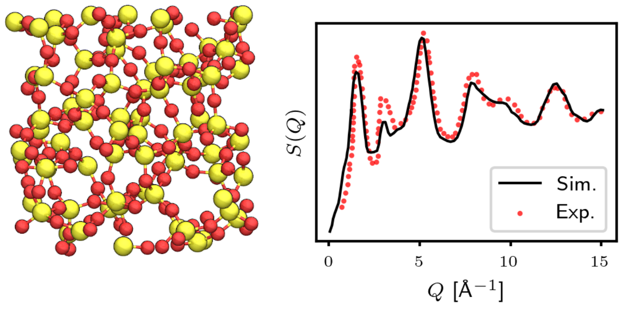
Fig. 1: Left: An example of an atomistic model structure for amorphous
SiO2 containing 216 atoms. Right: The validity of the atomistic models is verified by comparing the theoretical structure factor S(Q) of the model to experimental data.
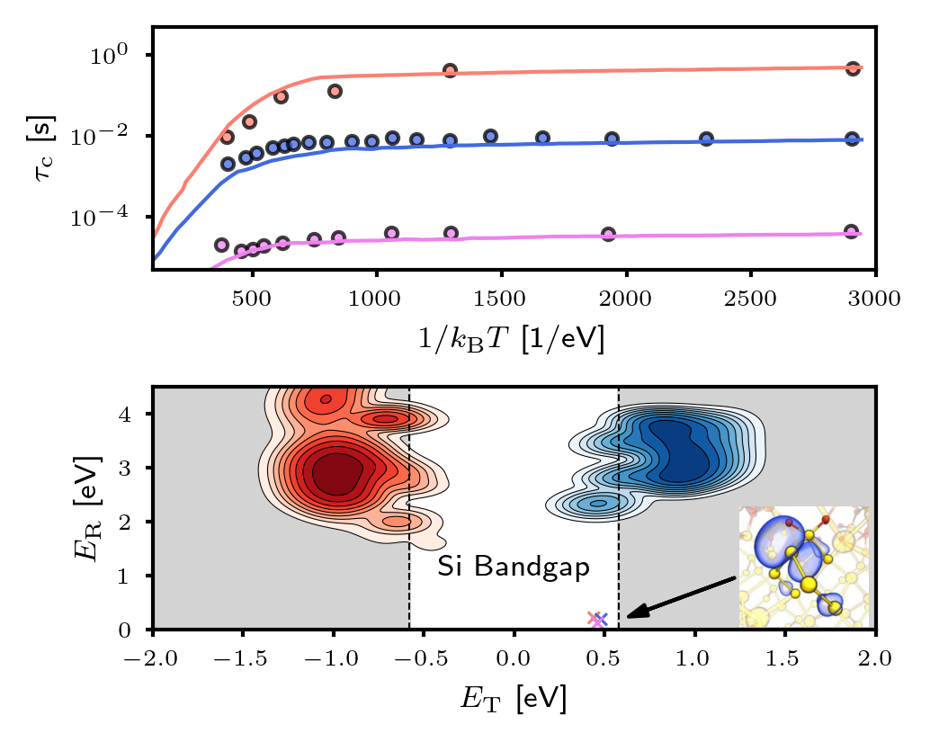
Fig. 2: Top: Experimental capture time constants τc for three defects (dots) as extracted from RTN measurements at cryogenic temperatures (4 K to 30 K) and the corresponding model predictions (lines). Bottom: The required defect parameters (crosses) to describe the charge trapping behavior are vastly different from typical parameter distributions for hole (red) or
electron (blue) traps in a-SiO2. Instead, the observed defect parameters
match the canonical Pb-center at the Si/SiO2 interface (inset), making it a
likely cause for noise in the studied devices.