
 |
|
||||
BiographyChristoph Wilhelmer was born 1993 in Lienz, Austria. He received his Bachelor degree in Technical Physics from TU Wien after doing an exchange semester at the University of Bath, UK in 2017. He received his Diplom-Ingenieur degree in Technical Physics from TU Wien in 2020 where he carried out his Master Thesis in the Quantum Materials group of the Institute of Solid State Physics. In March 2020 he joined the Institute for Microelectronics where he started his PhD, focusing on defect creation mechanisms in oxides used for semiconductor applications. |
|||||
Electron Polarons in Amorphous Hydrogenated Silicon Nitride (a-Si3N4:H)
In non-volatile memory devices such as charge trap flash, silicon nitride (Si3N4) is usually employed as the charge storage layer. This is motivated by the comparably high trap density (> 1019 cm-3) of this material, which originates from a large variety of electrically active defect sites, including dangling bonds (1016 cm-3 - 1018 cm-3), vacancies, and intrinsic trapping sites at overcoordinated atoms. Furthermore, silicon nitrides exhibit high H concentrations, which may lead to additional trapping centers. On the other hand, H also passivates most of the Si and N dangling bonds (~ 1022 cm-3 Si—H and N—H). The high trap concentration is thus expected to correspond to intrinsic trapping sites or polarons, which have been detected in amorphous materials such as SiO2 and HfO2.
Here, we conduct ab initio investigations in amorphous hydrogenated silicon nitride a-Si3N4:H to detect and analyze electron polaron sites, which are suspected to be responsible for the memory effect in the charge trapping layers of charge trap flash (CTF) devices. The investigated sample structures are created with a melt-and-quench procedure, employing a machine-learned force field trained on density functional theory (DFT) calculations of more than 1600 structures. Subsequently, the dangling bonds are passivated with H and relaxed in the negative and neutral charge states to investigate charge localization at specific precursor sites. The resulting structures have no dangling bonds or defect states in the band gap. They agree with experimental perceptions, including coordination number, electronic band gap, and structure factor. To quantify the localization of molecular orbitals (MOs), the inverse participation ratio was calculated and is shown for a sample structure in Fig. 1. From this plot, it can easily be seen that states near the band edges have a higher degree of localization than states deeper in the band and can thus potentially act as precursor sites for charge trapping.
Indeed, by relaxing the structures in the negative charge state, we find that an added electron gets preferably trapped at these localized precursor sites. The precursor sites can be identified as stretched Si—N bonds in the amorphous network, typically around 0.15 Å longer than the peak of the total Si—N distribution. The atomic structure of such a trapping site is shown in Fig. 2 in the neutral (left) and negative (right) charge state, with the localized lowest unoccupied MO (LUMO, neutral) and highest occupied MO (HOMO, negative) drawn as blue bubbles. The corresponding projected density of states (PDOS) is plotted below. When an electron gets trapped near the prolonged Si—N bond, it is further stretched by 0.43 Å on average, and the electronic state at the conduction band, now occupied, is shifted towards the middle of the band gap due to electronic relaxations. We also find that the thermodynamic charge transition levels of the electron polarons are within the band gap, and the relaxation energies upon electron trapping are distributed above 1.3 eV. Thus, we argue that stretched Si—N bonds can be considered as suitable electron trapping sites to explain the memory effect in CTFs.
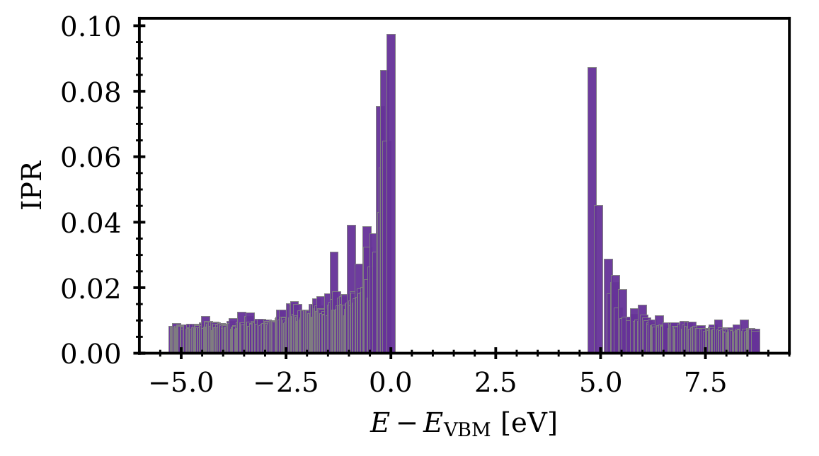
Fig. 1: Electronic inverse participation ratio (IPR) of an a-Si3N4:H structure near the band gap. Energies are given with respect to the valence band maximum (VBM).
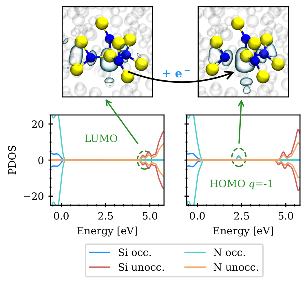
Fig. 2: Top: LUMO of neutral a-Si3N4:H (left) and HOMO of the negatively charged Si3N4:H after trapping an electron (right). Bottom: Projected density of states (PDOS) of neutral (left) and negatively charged a-Si3N4 with an occupied defect state in the band gap (right). Positive and negative PDOS values correspond to spin states up and down, respectively.