 |
|
Biography
Hajdin Ceric was born in Sarajevo, Bosnia and Herzegovina, in 1970. He studied electrical engineering at the Electrotechnical Faculty of the University of Sarajevo and the Technische Universität Wien, where he received the degree of Diplomingenieur in 2000. In June 2000, he joined the Institute for Microelectronics, where he received the doctoral degree in technical sciences in 2005 and where he is currently employed as a post-doctoral researcher. His scientific interests include interconnect and process simulation.
Compact Modeling of Electromigration in 3D ICs
ElectroMigration (EM) models can be generally divided into two types of models: full physical models and compact models. The full physical model is defined by a set of Partial Differential Equations (PDEs). It describes a degradation process of metallic interconnect under the influence of EM for an arbitrary three-dimensional interconnect geometry.
State-of-the-art EM models are capable of predicting a development of EM failure for a wide spectrum of operating conditions. An application of full physical EM models demands numerical solving of the model’s PDEs by a simulation tool. The handling of an EM model demands expert knowledge of EM models, numerical procedure, and the applied simulation tool. For these reasons, and due to the fact that full physical simulation may demand several hours of simulation time, the application of compact models is very practicable. The compact model is a set of one or more analytical expressions which enable a calculation of one or more values relevant for the determination of the state of the test unit (interconnect). The design and derivation of a compact model is carried out based on the following: study of theoretical-analytical models, simulations based on full physical models, experimental results, and observations. A single compact model is more applicable for a smaller group of problems than the full physical model. Typically a compact model describes the behavior of the reliability relevant characteristics of interconnect test unit for varying operating conditions. For a different layout, technology process, material choice, and geometry – a new compact needs to be constructed. The current focus of my work is the development of compact models for the most important reliability issues of modern 3D interconnects: Failure of solder bumps and Through Silicon Vias (TSVs).
Compact reliability models are calibrated and tested using experimental results provided by industrial partners.
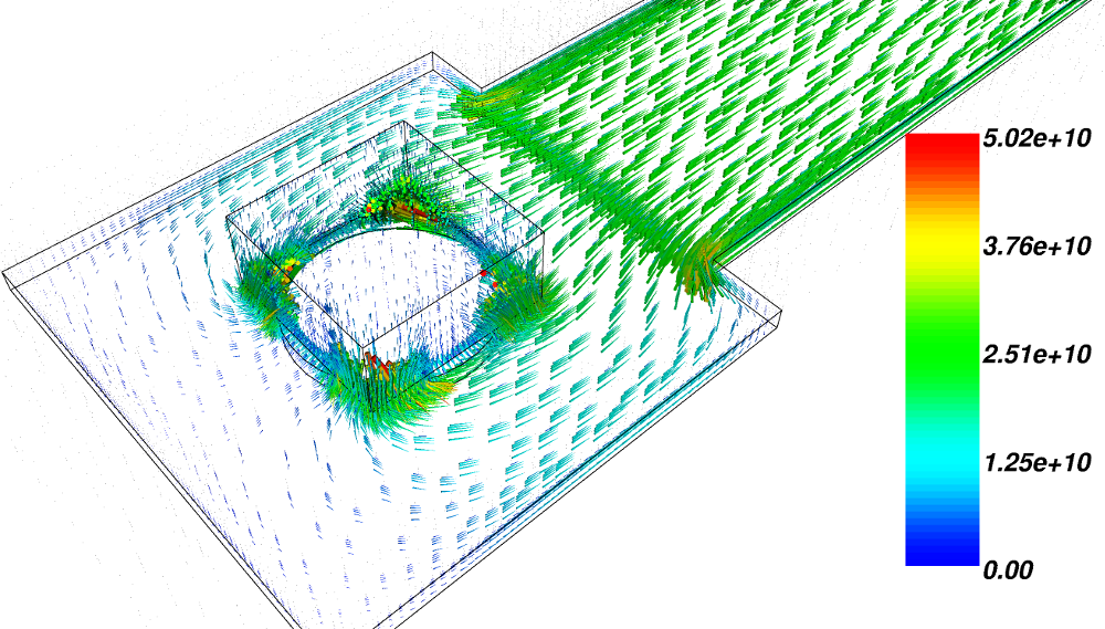
Fig. 1: Electron current density distribution (in A/m2) under the TSV in the presence of a void. Current crowding towards the corners of the via can be seen.