 |
|
Biography
Lidija Filipovic was born in Sarajevo, Yugoslavia in 1982. She studied electrical engineering at Carleton University, in Ottawa, Canada, where she received the degree of Bachelor in Electrical Engineering in 2005 and Master of Applied Science in 2007. She joined the Institute for Microelectronics in March 2012, where she is currently working on her doctoral degree. Her scientific interest is focused on nanowire heterostructures and device simulation.
Band-to-Band Tunneling in 3D Devices
Tunneling devices have shown clear promise in providing a steep subthreshold swing, garnering much interest for ultra low power switching applications. In order to study the tunneling in realistic devices, it is necessary to consider a full three-dimensional (3D) approach. In our work we expand on a recently proposed method to compute band-to-band tunneling currents in 3D structures.
Typically, the Wentzel–Kramers–Brillouin (WKB) approach is used to estimate the transmission coefficient from parameters that are extracted from the energy bands. Some improvements to this approach have been suggested recently. However, these methods approximate the effective mass and extract linearized band parameters. The effect of the masses in valence and conduction bands need to be considered in a more consistent manner, as their effect on tunneling differs depending on the device and material properties. The method developed through this work does not make such WKB-like assumptions. A propagating wave is computed using an approach based on the quantum-transmitting boundary method. The effective mass and energy barrier are treated as parameters varying between the valence and conduction band values. Our method computes tunneling through an effective barrier between the energy bands.
We have used this model for the study of i-Si/n-InAs heterojunctions, which are investigated for tunneling applications. Contrary to Silicon, which is an indirect bandgap material, and as such, requires phonon interaction to assist the tunneling process, Si/III-V junctions achieve a direct bandgap. In order to decrease the effects of dislocations in the heterojunction, we simulate various device configurations that would move the tunneling location away from the physical interface.
By adding gate overlap and inserting an undoped InAs segment, we have demonstrated that the tunneling barrier can be shifted away from the physical interface. The simulated devices are compared with a fabricated device by comparing the tunneling current (see Fig. 1). As expected, the initial device results in an overestimation of tunneling current, as only the ideal direct tunneling is considered. Gate overlap moves the tunneling barrier away from the physical interface, and decreases the tunneling current. The alternative device configuration of i-Si/i-InAs/n-InAs, moves the tunneling barrier while resulting in a larger tunneling current.
This method provides new insight into Band-To-Band (BTB) tunneling in real devices, as the computation considers 3D variations in material properties, electrostatic potential, and geometry. The visualization of an effective BTB tunneling barrier allows for a better understanding of wave propagation. With this knowledge, tunneling device improvements and optimizations are possible. This study demonstrates the value of 3D simulations of tunneling devices in order to investigate various segment configurations. The computed 3D tunneling barrier responds naturally to changes in device geometry, material parameters and applied bias. The flexibility of this approach could further be exploited to minimize the challenges faced by novel devices and material combinations.
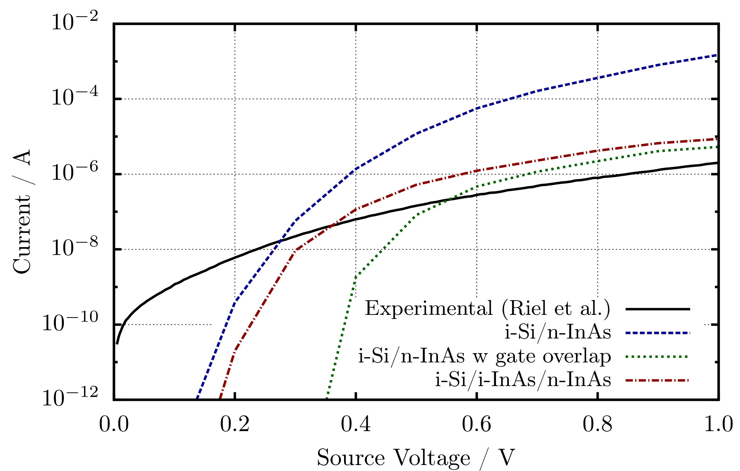
Fig. 1: Current-voltage characteristics of the investigated alternative heterostructure Tunneling FET designs compared to a manufactured reference device.