
 |
|
Biography
Joydeep Ghosh was born in Kolkata, India. He studied electrical engineering at the Jadavpur University, Kolkata. He was in IBM India Pvt. Ltd. for almost 3 years. Then he studied masters in "Micro and Nano Science" at the Technical University of Chemnitz, Germany, where he completed his studies in 2011. He joined the Institute for Microelectronics in March 2012. His current scientific interests include the spin injection and transport model in silicon.
Reduction of the Intersubband Spin Relaxation and Enhancement of the Spin Lifetime in Strained-SOI Films
Silicon is an ideal material for the spin-driven applications due to its long Spin Lifetime (SL). Considerable spin relaxation in gated silicon structures was experimentally observed, and several orders of magnitude boost of SL in (0 0 1) thin films subjected to [1 1 0] uniaxial tensile stress was predicted. We highlight the physical reasons behind the enhancement of SL. It is mentioned that spin-flip scattering processes between the two unprimed [0 0 1] valleys are primarily responsible for spin relaxation in our sample. We obtain the electron subband energies and the wave functions with the two-band k·p spin-Hamiltonian describing the valley dispersion, provided the confinement potential is an infinite square well. We consider the surface roughness and the longitudinal and transversal acoustic phonons to cause the prominent spin relaxation mechanisms. First it is assumed that the spin is injected along the perpendicular OZ-axis. Fig. 1 depicts that the spin relaxation rate with applied stress is highly reduced, and hence SL is increased by orders of magnitude. Fig. 1 also demonstrates how SL drops at elevated temperature because of the increased phonon scattering rate. We notice that at low to intermediate stress the major contribution to spin relaxation comes from the intersubband processes, whereas at higher stress the intrasubband component also becomes non-negligible. We confirm that the shear stress introduces a splitting between the usually considered unprimed subbands to increase the spin lifetime in silicon.
We further investigate whether spin injection orientation has any additional impact on SL. As already reported for bulk silicon, we show in Fig. 2 for our thin film that a change of the spin injection orientation from perpendicular (OZ-axis)- to in-plane (OX-axis) further reduces (enhance) the spin scattering (lifetime) over a wide range of the applied stress.
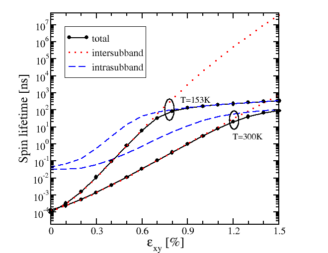
Fig. 1: Spin lifetime and its components with stress for a sample thickness of 1.36nm.
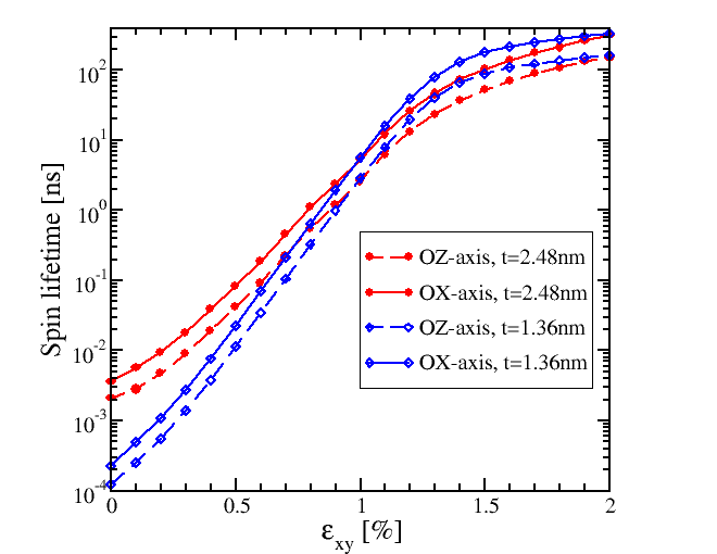
Fig. 2: Injection direction sensitive spin lifetime with stress at T=300K.