 |
|
Biography
Hans Kosina received the Diplomingenieur degree in electrical engineering and PhD from the Technische Universität Wien in 1987 and 1992, respectively. He was with the Institute of Flexible Automation at the Technische Universität Wien for one year and then joined the Institute for Microelectronics, where he is currently an Associate Professor. He received the venia docendi in microelectronics in 1998. In the summer of 1993, he was a visiting scientist at Motorola Inc., Austin, Texas, and in the summer of 1999, a visiting scientist at Intel Corp., Santa Clara, California. Dr. Kosina served as a Technical Program Committee member in the IEEE International Workshop on Computational Electronics in 2003 and 2004 and was the chairman of the ''11th International Workshop on Computational Electronics'' held in Vienna in May 2006. He has served as the Associate Editor of the IEEE Transactions on Computer-Aided Design of Circuits and Systems since January 2004. His current research interests include the device modeling of semiconductor devices, nanoelectronic devices, organic semiconductors and optoelectronic devices, the development of novel Monte Carlo algorithms for classical and quantum transport problems, and computer-aided engineering in ULSI-technology.
Electronic Transport in Semiconductor Nanostrucutures
Our simulators for electronic transport in semiconductor nanostructures have been enhanced further and applied to various technologically relevant devices and structures. Based on the linearized Boltzmann equation, two problems have been addressed. First, the mobility in ultra-narrow, non-planar channels has been analyzed, taking into account the full-band-structure (Fig. 1). The design space of non-planar channels - including the cross section shape, channel orientation, and strain - has been explored. Numerical methods to accelerate the full band mobility calculations have been developed. Second, the low-field mobility of single MoS2 layers has been analyzed. The electronic structure has been obtained from ab-initio calculations. The transport study takes into account electron scattering due to intra-valley and inter-valley acoustic phonons, optical and polar optical phonons, remote phonons, and charged impurities. Dynamic screening for phonons and static screening for charged impurities is assumed. The dependences of mobility on strain and also on the dielectric material have been studied. Ballistic quantum transport models available in the Vienna Schrödinger Poission Solver (VSP) are the Quantum Transmitting Boundary Method (QTBM) and the Non-equilibrium Green's Function method (NEGF). The former method has been employed to study interband tunneling devices. For the study of nanowire tunnel FETs, a full three-dimensional (3D) QTBM approach has been implemented. The model has been used to investigate i-Si/i-InAs/n-InAs heterojunctions for tunneling applications. In this structure, the tunneling barrier moves away from the physical Si interface, and tunneling takes place in the direct semiconductor. In this way, a larger tunneling current is obtained. Furthermore, the QTBM has been used to investigate the quantum transport properties of nanoscaled high-frequency GaN High-Electron Mobility Transistors. For that purpose, unstructured grids in arbitrary dimension (1D/2D/3D) and arbitrary crystal orientations have been made available in VSP. The model allows for a consistent treatment of size quantization and transport effects. The electron concentration, conduction bandedges and ballistic current through the device have been calculated self-consistently, assuming both a strained and unstrained GaN/AlGaN heterostructure. Due to a larger interface charge in the fully strained device, stronger confinement is achieved, whereas in the relaxed device the current is partly flowing through the back barrier region.
Energy filtering in nanostructured thermoelectrics has been studied using fully dissipative quantum transport calculations. The NEGF model used includes scattering from both acoustic and optical phonons. A promising way to improve the thermoelectric efficiency of a semiconductor is the introduction of a grating of potential barriers. Such barriers could be the result of nanogranularity, with the grain boundaries acting as barriers, or the result of the creation of a superlattice. We have been studying both the effects that the shape and size of these barriers have on the thermoelectric figure of merit, ZT, and the sensitivity of the improvement to random variation and non-idealities in the barrier grating. It is important both to understand how effective these barriers can be and how feasible their use is within realistic structures.
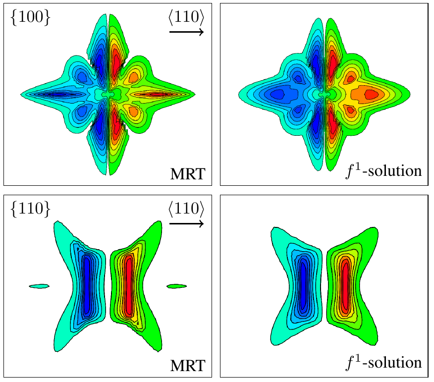
Fig. 1: Response of the hole distribution function for {100} and {110}-oriented p-type MOS channels. The left pictures show the response in the Microscopic Relaxation Time (MRT) approximation, the right pictures show the result from the linearized Boltzmann equation. The coupling among subbands causes a redistribution of carriers not seen in the MRT picture.