 |
|
Biography
Santo Papaleo was born in Novara, Italy, in 1988. He received the bachelor's degree in material science at the Università degli Studi del Piemonte-Orientale, and he received the master's degree in material science at the Università degli Studi di Milano-Bicocca in 2013. He joined the Institute for Microelectronics in 2013, where he is currently working on his doctoral degree. His scientific interests include stress estimation in TSV.
Study Delamination at the Bottom of TSVs
Through Silicon Vias (TSVs) are a part of the interconnects for three-dimensional (3D) technology and are the units that establish the connection through silicon die. This technology has become necessary to maintain the performance increase of integrated circuits described by Moore law. The usage of this new technology creates new mechanical reliability problems. We are studying open TSVs that have a cylindric structure, which is coated rather than entirely filled with the conducting metal. The investigations regarding the mechanical reliability are performed at the bottom of the TSV. The bottom consists of different material layers with different thicknesses and mechanical properties. In these interfaces the possibility of delamination leading to the failure of the devices needs to be considered. The prediction of delamination is analyzed employing the J-integral method. Values of J-integral correspond to the Energy Release Rate (ERR). ERR is the energy dissipated during delamination and it is defined as the energy per unit of created fracture length. Using the finite element method, the J-integral is calculated for different predefined crack lengths. The simulation permits to change the initial stresses, thicknesses, and external force of the system.
These factors are related to the technology process. It is possible to calculate the ERRs for different interfaces and different boundary conditions, and compare them with critical ERRs, which are available in literature. Fig. 1 shows the results at the interface SiO2/W, where the critical ERR is 0.2-0.5J/m2. It illustrates how different values of initial stress in W change the ERR as a function of a/w (crack length/layer length) ratio beyond 1.25GPa (which is the critical ERR), thus leading to delamination. This analysis permits prediction of an influence of the mechanical and geometrical parameters on the delamination probability in the considered system, and these results are useful for design optimization regarding the reduction of delamination in TSVs.
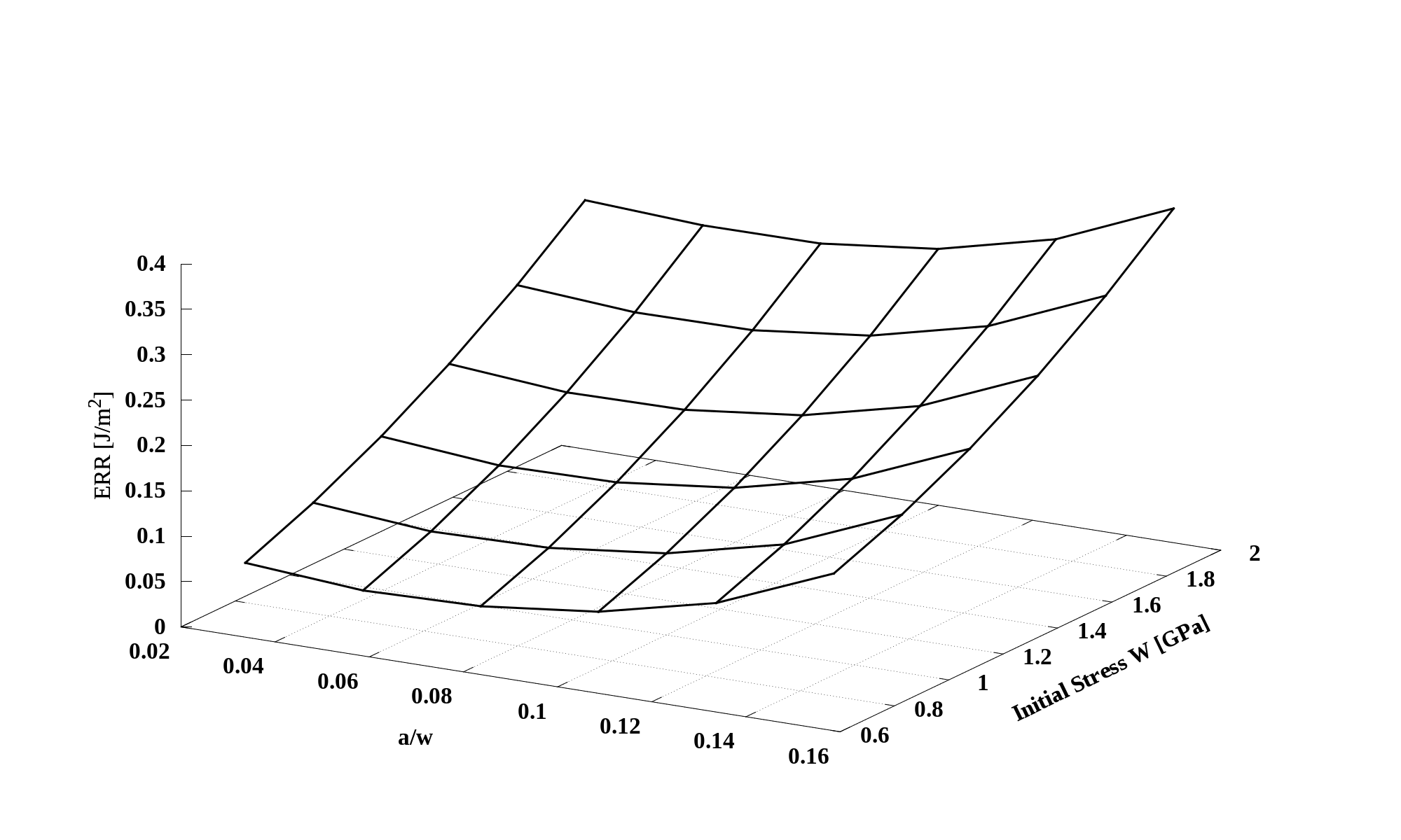
Fig. 1: The ERR for different initial stresses and crack lengths in the SiO2/W interface.